SG3225HBN (Crystal Oscillator )
- Frequency range
100MHz to 325MHz - Supply voltage
2.5V, 3.3V - Output
HCSL - Function
Output enable (OE) - External dimensions
3.2 × 2.5 × 1.05mm - Phase jitter
85 fs Typ (f0 = 156.25MHz)
(High-Frequency Fundamental)
![]()
![]()

SG3225HBN
Design Support Data Download
Specifications
| Item | Symbol | Specifications | Conditions / Remarks |
|---|---|---|---|
| Output frequency range | f0 | 100MHz to 325MHz | Please contact us for inquiries regarding available frequencies. |
| Supply voltage | VCC | D:2.5V ±0.125V, C:3.3V ±0.165V | |
| Storage temperature | T_stg | -55℃ to +125℃ | Store as bare product. |
| Operating temperature | T_use | G: -40℃ to +85℃, H: -40℃ to +105℃ | |
| Frequency tolerance | f_tol | J: ± 50 × 10-6 (Not available H: -40℃ to +105℃) |
Includes initial tolerance, temperature change, Vcc change and 10 years aging(+25 °C) |
| L: ± 100 × 10-6 | Includes initial tolerance, temperature change, Vcc change and 10 years aging(+25 °C) |
||
| Current consumption | ICC | 25 mA Typ. , 35mA Max. | OE=VCC,with output load |
| Disable current | I_dis | 15mA Max. | OE=GND |
| Symmetry | SYM | 45% to 55% | At outputs crossing point |
| Output voltage | VOH | 0.75 V Typ., 0.66V to 0.85V | DC characteristics, single output |
| VOL | 0 V Typ., -0.15V to 0.15V | ||
| Crossing voltage | VCR | 0.25V to 0.55V | |
| Output load condition | L_HCSL | 50Ω | |
| RS | 33Ω | ||
| Input voltage | VIH | 70% VCC Min. | OE terminal |
| VIL | 30% VCC Max. | ||
| Differential output rise slew rate/ fall slew rate |
Rr / Rf | 1 V/ns to 4V/ns | Between -0.15 V and 0.15 V of differential output |
| Start-up time | t_str | 10ms Max. | Time at minimum supply voltage to be 0 s |
Phase Jitter
| Output frequency |
100 MHz | 125 MHz | 156.25 MHz | 200 MHz | 322.265625 MHz | Supply voltage | |
|---|---|---|---|---|---|---|---|
| Phase Jitter [fs] Offset Frequency 12 kHz to 20MHz |
Typ. | 110 | 95 | 85 | 75 | 65 | 3.3V ± 0.165V |
| Max. | 180 | 160 | 140 | 125 | 110 |
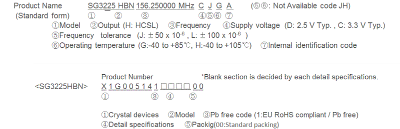
External dimensions
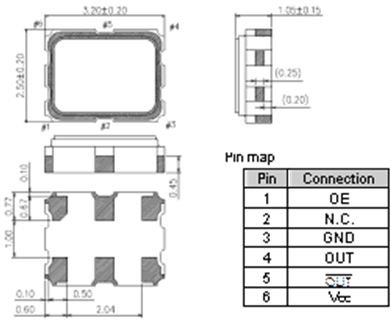
(Unit: mm)
- OE pin = HIGH : Specified frequency output.
- OE pin = LOW : Output is high impedance.
Footprint (Recommended)
(Unit: mm)
In order to achieve optimum jitter performance,
it is recommended that the capacitor (0.1 μF + 10 μF)
between Vcc and GND pin should be placed as close to
the Vcc pin as possible.
