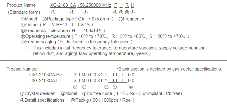
XG-2103CA (Crystal Oscillator Low-Jitter SAW Oscillator)
- Frequency range100MHz to 700MHz
- Supply voltage
3.3V Typ.
- Output LV-PECL or LVDS
- Function Output enable (OE)
- External dimensions 7.0 × 5.0 × 1.2mm
- Low jitter and low phase noise by SAW unit.
![]()
![]()

XG-2103CA
Specifications
| Item | Symbol | LV-PECL | LVDS | Conditions/ Remarks |
||
|---|---|---|---|---|---|---|
| XG-2103CA P | XG-2103CA L | |||||
| Output frequency range | f0 | 100MHz to 700MHz | Please contact us for inquiries regarding available frequencies. | |||
| Supply voltage | VCC | 3.3V ± 0.33V | ||||
| Storage temperature | T_stg | -55°C to +125°C | Store as bare product. | |||
| Operating temperature | T_use | P : 0°C to +70°C R : -5°C to +85°C S : -20°C to +70°C |
||||
| Frequency tolerance | f_tol | H : ±100 × 10-6 | ||||
| Current consumption | ICC | 60mA Max. | - | OE = VCC , L_ECL = 50Ω | ||
| - | 30mA Max. | OE = VCC , L_LVDS = 100Ω | ||||
| Disable current | I_dis | 2mA Max. | 15mA Max. | OE = GND | ||
| Symmetry | SYM | 45% to 55% | At outputs crossing point | |||
| Output voltage (LV-PECL) |
VOH | 2.35V Typ. | - | DC characteristics | ||
| VCC - 1.025V to VCC - 0.88V | - | |||||
| VOL | 1.60V Typ. | - | ||||
| VCC - 1.81V to VCC - 1.62V | - | |||||
| Output voltage (LVDS) |
VOD | - | 350mV Typ, 247mV to 454mV |
VOD1 , VOD2 | DC characteristics | |
| dVOD | - | 50mV Max. | dVOD = | VOD1 - VOD2 | | |||
| VOS | - | 1.25V Typ, 1.125V to 1.375V |
VOS1 , VOS2 | |||
| dVOS | - | 150mV Max. | dVOS = | VOS1 - VOS2 | | |||
| Output load condition (ECL) / (LVDS) |
L_ECL | 50Ω | - | Terminated to VCC - 2.0V | ||
| L_LVDS | - | 100Ω | Connected between OUT to OUT | |||
| Input voltage | VIH | 70% VCC Min. | OE terminal | |||
| VIL | 30% VCC Max. | |||||
| Rise time / Fall time | tr / tf | 400ps Max. | Between 20% and 80% of ( VOH - VOL) Between 20% and 80% of Differential Output peak to peak voltage |
|||
| Start-up time | t_str | 10ms Max. | Time at minimum supply voltage to be 0s | |||
| Phase Jitter | tPJ | 0.23ps Max. | 0.27ps Max. | 100MHz ≦ f0 < 150MHz | Offset frequency: 12kHz to 20MHz |
|
| 0.22ps Max. | 0.24ps Max. | 150MHz ≦ f0 < 200MHz | ||||
| 0.21ps Max. | 0.23ps Max. | 200MHz ≦ f0 < 300MHz | ||||
| 0.18ps Max. | 0.19ps Max. | 300MHz ≦ f0 < 400MHz | ||||
| 0.16ps Max. | 0.16ps Max. | 400MHz ≦ f0 < 500MHz | ||||
| 0.14ps Max. | 0.14ps Max. | 500MHz ≦ f0 < 600MHz | ||||
| 0.10ps Max. | 0.10ps Max. | 600MHz ≦ f0 < 700MHz | ||||
| Frequency aging | f_aging | H : Included in Frequency tolerance | Max operating temperature , 5years , VCC = 3.3V | |||
External dimensions
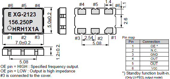
(Unit: mm)
Footprint (Recommended)
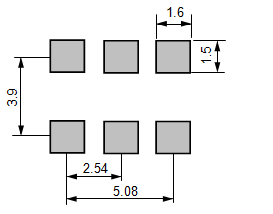
(Unit: mm)
To maintain stable operation, provide a 0.01 µF to 0.1 µF by-pass capacitor at a location as near as possible to the power source terminal of the crystal product (between VCC - GND).
