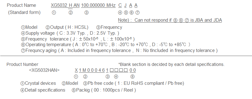
XG5032HAN (Crystal Oscillator Low-Jitter SAW Oscillator)
- Frequency range100MHz to 200MHz
- Supply voltage 2.5V Typ. / 3.3V Typ
- Output HCSL
- Function Output enable (OE)
- External dimensions 5.0 × 3.2 × 1.4mm
- Low jitter and low phase noise by SAW unit.
![]()
![]()

XG5032HAN
Specifications
| Item | Symbol | Specifications | Conditions / Remarks | |
|---|---|---|---|---|
| Output frequency range | f0 | 100MHz to 200MHz | Please contact us for inquiries regarding available frequencies. | |
| Supply voltage | VCC | C : 3.3V ± 0.33V D : 2.5V ± 0.125V |
||
| Storage temperature | T_stg | -55°C to +125°C | Store as bare product. | |
| Operating temperature *1 | T_use | A : 0°C to +70°C B : -20°C to +70°C D : -5°C to +85°C |
||
| Frequency tolerance *1 | f_tol | J : ± 50 × 10-6 L : ±100 × 10-6 |
||
| Current consumption | ICC | 35mA Max. | OE = VCC , with output load | |
| Disable current | I_dis | 15mA Max. | OE = GND | |
| Symmetry | SYM | 45% to 55% | at outputs crossing point | |
| Output voltage | VOH | 0.75 V Typ. , 0.66V to 0.85V | DC characteristics,Single output | |
| VOL | 0 V Typ. , -0.15V to 0.15V | |||
| Crossing Voltage |
Vcr | 0.25V to 0.55V | ||
| Input voltage | VIH | 70% VCC Min. | OE terminal | |
| VIL | 30% VCC Max. | |||
| differential output rise slew rate/ fall slew rate |
Rr / Rf | 1V/n to 4V/ns | Between -0.15% and 0.15 defferential output | |
| Start-up time | t_str | 10ms Max. | Time at minimum supply voltage to be 0s | |
| Phase Jitter | tPJ | 0.3ps Max. | f0 ≦ 160 MHz | Offset frequency: 12kHz to 20MHz |
| 0.4ps Max. | 160 MHz < f0 ≦ 175 MHz | |||
| 0.2ps Max. | f0 > 175 MHz | |||
| Frequency aging | f_aging | ± 10 × 10-6 / year Max. | First year | +25°C ,
First year VCC = 2.5V , 3.3V |
| A : Included in Frequency tolerance | 10years | |||
Measurement circuit
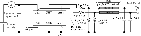
By-pass capacitor 1 (approx. 0.01µF to 0.1 µF) places closely between Vcc and GND.
By-pass capacitor 2 (approx. 10 µF) places closely between power supply terminals on the board.
Output line length L is estimated as follows
![]()
External dimensions
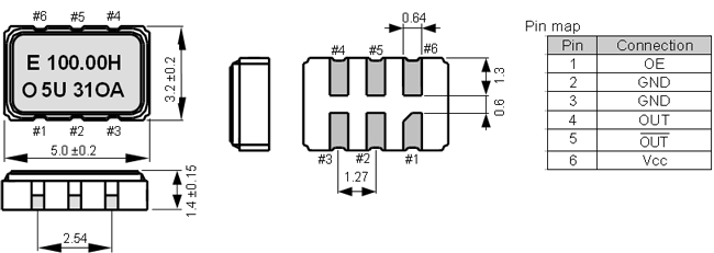
(Unit: mm)
OE pin = HIGH : Specified frequency output.
OE pin = LOW : Output is high impedance #2 and #3 are connected to the cover.
Footprint (Recommended)
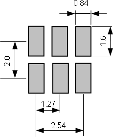
(Unit: mm)
To maintain stable operation, provide a 0.01uF to 0.1uF by-pass capacitor at a location as near as possible to the power source terminal of the crystal product (between Vcc - GND).
