- RTC Top
- What is RTC Modules?
- Epson's RTC Modules
- Features
- Scenes
- RTC Modules for Automotive
- Development Tools
- Videos
RA8803SA for Automotive
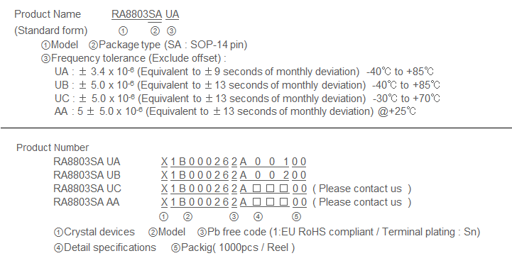
(Built-in 32.768kHz-DTCXO, High Stability I2C-Bus Interface Real Time Clock Module)
- Built in frequency adjusted 32.768kHz crystal unit and DTCXO.
- 1/100s resolution Time register
- Interface Type
I2C-Bus interface (400kHz)
- Interface voltage range
1.6V to 5.5V
- Temp. compensated voltage range
2.2V to 5.5V
- Timekeeping voltage range
1.6V to 5.5V
- Selectable clock output (32.768kHz, 1024Hz, 1Hz)
- The various functions include full calendar, alarm, timer, EVIN input.
- Applications: Car audio, Car navigation system, Clock.
- AEC-Q200 compliant
![]()
![]()

RA8803SA
Application Manual
(ETM39E-03) ![]() (991kB)
(991kB)
Design Support Data Download
Block diagram
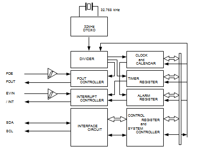
Overview
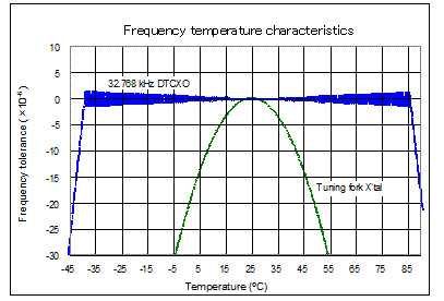
- High Stability
- UA ± 3.4 × 10⁻⁶ / -40°C to +85°C
- (Equivalent to ±9seconds of month deviation)
- UB ± 5.0 × 10⁻⁶ / -40°C to +85°C
- (Equivalent to ±13seconds of month deviation)
- UC ± 5.0 × 10⁻⁶ / -30°C to +70°C
- (Equivalent to ±13seconds of month deviation)
- AA (+5 ± 5.0) × 10-6 / +25°C
- High Resolution:1/100s Time register with capture buffer
- 32.768kHz frequency output function
- FOUT pin output (C-MOS output), CL=30pF
- Output selectable: 32.768kHz, 1024Hz, 1Hz
- The various interrupt
- Timer Function can be set between 1/ 4096second and 4095minutes.
- Alarm Function can be set to day of week, day, hour, or minute.
- EVIN input.
- Time synchronize function with 1PPS signal input
- Register compatibility: upper compatible with RX-8801.
- *It is possible to use it by the terminal connection as 32.768kHz-DTCXO.
Specifications *Refer to application manual for details.
Electrical Characteristics
| Item | Symbol | Condition | Min. | Typ. | Max. | Unit | |
|---|---|---|---|---|---|---|---|
| Operating voltage | VDD | Interface voltage | 1.6 | 3.0 | 5.5 | V | |
| Temp. compensated Voltage | VTEM | Temp. compensated voltage | 2.2 | 3.0 | 5.5 | V | |
| Clock supply voltage | VCLK | - | 1.6 | 3.0 | 5.5 | V | |
| Operating temperature | TOPR | -40 | +25 | +85 | °C | ||
| Stability | Δf/f | UA | Ta = -40°C to +85°C | ±3.4*1 | ×10-6 | ||
| UB | Ta = -40°C to +85°C | ±5.0*2 | |||||
| UC | Ta = -30°C to +70°C | ||||||
| AA | Ta = +25°C | 5 ± 5.0*3 | |||||
| Current consumption (1) | IDD1 | Backup Mode FOE = GND, /INT = VDD FOUT output : OFF |
VDD = 5V | - | 0.75 | 3.4 | µA |
| Current consumption (2) | IDD2 | VDD = 3V | - | 0.75 | 2.1 | ||
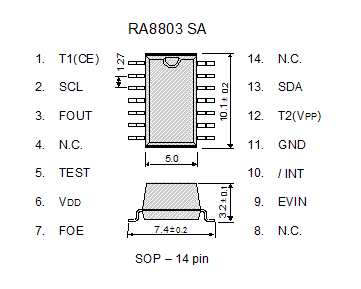
Pin function
| Signal Name | Input/Output | Function |
|---|---|---|
| T1(CE) | Input | Use by the manufacture for testing. ( Do not connect externally.) |
| SCL | Input | Serial clock input pin. |
| FOUT | Output | The pin outputs the reference clock signal. ( CMOS output ) |
| TEST | Input | Use by the manufacture for testing. ( Do not connect externally. RX-8803SA only.) |
| VDD | - | Connected to a positive power supply |
| FOE | Input | The input pin for the FOUT output control. |
| EVIN | Input | External event input. ( Do not make this pin OPEN.) |
| / INT | Output | Interrupt output (N-ch. open drain). |
| GND | - | Connected to a ground |
| T2(VPP) | - | Use by the manufacture for testing. ( Do not connect externally.) |
| SDA | I/O | Data input and output pin. |
Terminal connection / External dimensions
(Unit: mm)
The metal case inside of the molding compound may be exposed on the top or bottom of this product.
This purely cosmetic and does not have any effect on quality, reliability or electrical specs.
Footprint (Recommended)
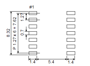
(Unit: mm)
To maintain stable operation, provide a 0.1uF by-pass capacitor
at a location as near as possible to the power source terminal of the crystal product (between Vcc - GND).
*1 Equivalent to 9 seconds of month deviation.
*2 Equivalent to 13 seconds of month deviation.
*3 Equivalent to 13 seconds of month deviation. (excluding offset)
32.768kHz-DTCXO Frequency temperature characteristics (Example)