- RTC Top
- What is RTC Modules?
- Epson's RTC Modules
- Features
- Scenes
- RTC Modules for Automotive
- Development Tools
- Videos
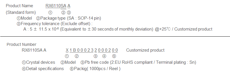
RX6110SA A (Real Time Clock Module Customized Product)
Power Switching and Low current consumption SPI & I2C-Bus
- Built in frequency adjusted 32.768 kHz crystal unit.
- Frequency tolerance
5±11.5x10⁻⁶ (Equivalent to ±30 seconds of monthly deviation/ Customized product)
- Interface Type
SPI-Bus & I2C-Bus
- Operating voltage range
1.6V to 5.5V
- The wide voltage for time keeping
1.1V to 5.5V
- Low backup current
170 nA / 3V(Typ.)
- Built-in RAM
Built-in 128 bit(8 bit × 16)RAM
- Auto power switching functions
When VDD deteriorates than 1.6V, internal source is switched to VBAT.
- The various functions include full calendar, alarm, timer.
- Epson prepared Linux driver for development
- https://www5.epsondevice.com/en/information/support/linux_rtc/
The registered trademark Linux® is used pursuant to a sublicense from LMI(Linux Mark Institute)
![]()

RX6110SA A
Application Manual
(ETM49E-01) ![]() (1.1MB)
(1.1MB)
Design Support Data Download
Block diagram
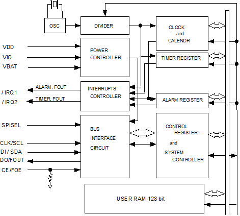
Overview
- Interface type.
- SPI-Bus and I2C-Bus interface.
- By a terminal, a switchover of the interface is possible.
- Built-in auto power switching function
- To efficiently charge from VDD to backup battery (Secondary battery, Large capacitor)
connected to VBAT is possible.
Detects VDD voltage drop(VDET-) and automatically switches to the backup battery.
- To efficiently charge from VDD to backup battery (Secondary battery, Large capacitor)
- Frequency output function
- Output frequency can be selected as 32.768kHz, 1024Hz, 1Hz.
- Timer function
- Timer function can be set up between 1/4096 second and 65535 hours.
- Timer source clock are 1hour, 1min, 64Hz, 4096Hz
- It is recorded automatic to TF-bit at the time of event occurrence, and possible to output with /IRQ1 or /IRQ2 pin.
- Alarm function
- Alarm function can be set to day of week, day, hour, and minute.
- It is recorded automatic to AF-bit at the time of event occurrence,
and possible to output with /IRQ1 pin output.
- Built-in RAM
- 128 bit (8 bit x 16, SRAM)
Specifications (characteristics)
*Refer to application manual for details.
Recommended Operating Conditions
| Item | Symbol | Conditions | Min. | Typ. | Max. | Unit |
|---|---|---|---|---|---|---|
| Power voltage | VDD | - | 1.6 | 3.0 | 5.5 | V |
| Clock voltage | VCLK | - | 1.1 | 3.0 | 5.5 | V |
| Operating temperature | TOPR | - | -40 | +25 | +85 | °C |
Frequency characteristics
| Item | Symbol | Conditions | Rating | Unit |
|---|---|---|---|---|
| Frequency tolerance | Δ f/f | Ta=+25°C VDD=3.0V |
A:5± 11.5*1) |
×10-6 |
| Oscillation start-up time |
tSTA | Ta=+25°C VDD=1.6V |
1 Max. | s |
*1) Equivalent to ±30 seconds of monthly deviation (excluding offset.)/ Customized product
Current consumption characteristics
*Ta=-40°C to+85°C
| Item | Symbo | Conditions | Min. | Typ. | Max. | Unit |
|---|---|---|---|---|---|---|
| Current Consumption | lBAK | VBAT=3.0V Input pins are "L" ,VDD = 0 V DO/FOUT=OFF, fCLK = 0 Hz, /IRQ1,2 = OFF, TSEL2="1" It include an OFF leak current of SW between the power supply (VBAT-VDD) |
- | 170 | 320 | nA |
| I32K | VDD=3.0V fCLK = 0 Hz,SPISEL=VIO, /IRQ1,2 = OFF, CE/FOE = VIO, DO/FOUT : 32.768 kHz ON , CL = 0 pF |
- | 1.5 | 2.1 | µA |
Pin Function
| Signal Name | Input/ Output |
Function |
|---|---|---|
| SPISEL | Input | The interface select pin.
SPI is chosen at a "H" level (VIO voltage) / I2C is chosen at a "L" level (GND voltage). |
| CE/FOE | Input | SPI: Should be held high to allow access to the CPU. Incorporates a pull-down resistor. I2C: It is an input pin for controlling the DO/FOUT output. When the frequency output from a DO/FOUT pin does not need, CE/FOE pin must be connected to GND. |
| CLK/SCL | Input | This is a shift clock input pin for serial data transmission. |
| DI/SDA | Input/ Output | SPI: This is the data input pin for serial data transfer. I2C: This is the data input/output pin for serial data transfer. |
| DO/FOUT | Output | SPI: This is the data output pin for serial data transfer. I2C: This is the C-MOS output pin with output control provided via the CE/FOE pin. (frequency selection: 32.768 kHz / 1024 Hz / 1Hz / Hi-z) |
| / IRQ1 | Output | This pin outputs interrupt signals ("L" level) for alarm, timer, time update, and FOUT.
This is an N-ch open-drain output. This pin can output even a backup mode. |
| / IRQ2 | Output | This pin outputs interrupt signals ("L" level) for timer and FOUT. This is an C-MOS output.
This pin becomes Hi-z in less than VDD=1.6V. |
| VDD | - | This is a power-supply pin. It can impress the voltage unlike VIO. |
| VIO | - | This pin is a power supply for input and the output and input / output pins.Connected to a positive power supply. |
| VBAT | - | Connect a secondary battery or capacitor for backup power supply.
If a backup power supply is not present, this pin connect to VDD. |
| GND | - | Connected to a ground. |
Terminal connection / External dimensions
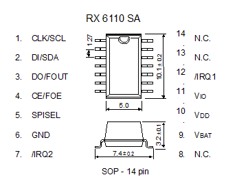
(Unit:mm)
The metal case inside of the molding compound may be exposed on the top or bottom of this product.
This purely cosmetic and does not have any effect on quality, reliability or electrical specs.
Footprint (Recommended)
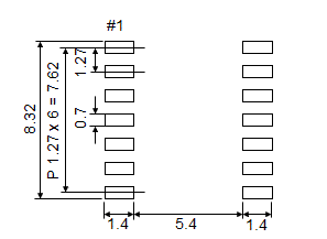
(Unit: mm)
To maintain stable operation, provide a 0.1uF by-pass capacitor
at a location as near as possible to the power source terminal of the crystal product (between Vcc - GND).
