- RTC Top
- What is RTC Modules?
- Epson's RTC Modules
- Features
- Scenes
- RTC Modules for Automotive
- Development Tools
- Videos
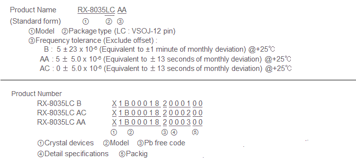
RX-8035LC (I2C-Bus Real Time Clock Module)
- Built in 32.768 kHz crystal unit
Frequency adjusted for high accuracy.(±5x10⁻⁶/Ta=+25°C)
- Interface Type
I2C-Bus Interface(400kHz)
- Operating voltage range
2.4V to 5.5V
- Wide voltage for Timekeeping
1.0V to 5.5V
- Low backup current
350nA(SA) 400nA(LC)/ 3V(Typ.)
- Event detection and Time stamp
One-shot full timestamp and interrupt.
- Dual event detection ports
Each terminal has a de-bounce circuit.
- Auto power switching functions
It switches VDD and VBAT, automatically
- Dual Alarm, Periodic interruption
- Epson prepared Linux driver for development
- https://www5.epsondevice.com/en/information/support/linux_rtc/
The registered trademark Linux® is used pursuant to a sublicense from LMI(Linux Mark Institute)
![]()

RX-8035LC
Block diagram
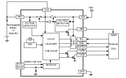
Overview
- The event detection and Timestamp function
- Dual event detection terminals.
- Selectable de-bounce period 35ms or 2s.
- Available event detection interrupt output.
- Power switching functions.
- An external diode is unnecessary to have a reverse current prevention switch built-in in
the VBAT side to connect a primary cell to. - When VDD is less than 2.4V, an internal source is switched to VBAT, and /RES is Low level.
When VDD voltage rises to higher than 2.52V, an internal source is switched to VDD, and /RES is released with 105ms delay. - Note: When the supply from VBAT, SCL and SDA are disabled.
- An external diode is unnecessary to have a reverse current prevention switch built-in in
- Alarm, Periodic interrupt, 32.768kHz clock output.
- Available monthly-alarm and weekly-alarm.
- Interrupt period are selectable from 2Hz to Monthly.
- CLKOUT outputs 32.768kHz clock powered by VDD.
Specifications (characteristics) *Refer to application manual for details.
Recommend Operating Conditions
| Item | Symbol | Conditions | Min. | Typ. | Max. | Unit |
|---|---|---|---|---|---|---|
| Operating voltage | VACCESS | VDD | 2.4 | 3.0 | 5.5 | V |
| Time keeping voltage | VCLK | VBAT | 1.0 | 3.0 | 5.5 | V |
| Operating temperature | TOPR | - | -40 | +25 | +85 | °C |
| Storage temperature | TSTG | - | -55 | - | +125 | °C |
Frequency characteristics
| Item | Symbol | Conditions | Rating | Unit |
|---|---|---|---|---|
| Frequency tolerance | Δ f/f | Ta=+25°C VBAT=3.0V |
B: 5±23 *1) AA: 5±5 *2) AC: 0±5 *2) |
×10-6 |
| Oscillation start-up time | tSTA | Ta=+25°C VDD=3.0V |
1 Max. | s |
| Frequency/voltage characteristics | f/V | Ta = +25°C VDD=2.4V to 5.5V |
±1 Max. | ×10-6 |
*1 Equivalent to ±1 minute of monthly deviation (excluding offset.)
*2 Equivalent to ±13 seconds of monthly deviation (excluding offset.)
Current consumption characteristics
Ta=-40°C to +85°C
| Item | Symbol | Conditions | Min. | Typ. | Max. | Unit |
|---|---|---|---|---|---|---|
| Current Consumption | lBAT | RX-8035SA VBAT=3.0V, VDD=0.0V SCL=SDA=GND |
- | 350 | 1200 | nA |
| RX-8035LC VBAT=3.0V, VDD=0.0V SCL=SDA=GND |
400 | |||||
| IDD | VDD=3.0V SCL=SDA=GND CLKOUT=open | - | 1.40 | 2.50 | µA |
Power supply detection voltage
Ta=-40°C to +85°C
| Item | Symbol | Condition | Min. | Typ. | Max. | Unit |
|---|---|---|---|---|---|---|
| VBAT detect voltage | VLOW | - | 1.10 | 1.25 | 1.40 | V |
| Power switching voltage (VDD to VBAT) |
VD2B | +25°C | 2.328 | 2.40 | 2.472 | V |
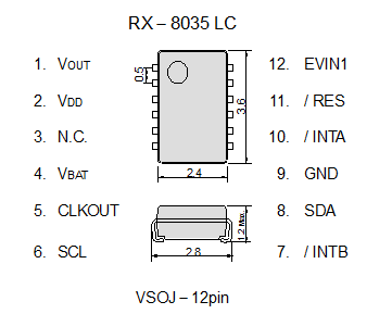
Pin function
| Signal Name | Input/Output | Functions |
|---|---|---|
| SCL | Input | I2C serial clock. |
| SDA | In/Out | I2C data in/out. |
| VDD | - | Main power supply. |
| VBAT | - | Power supply for backup. |
| Vout | Output | Switched power out.(maximum output current 20mA) |
| / RES | Output | VDD voltage state. |
| GND | - | Ground |
| EVIN1 | Input | Event detection input 1 |
| EVIN2 | Input | Event detection input 2 |
| / INTA | Output | Interrupt out A. |
| / INTB | Output | Interrupt out B. |
| CLKOUT | Output | 32.768kHz output. (CMOS. Can not inhibit.) |
| N.C. | - | Do not connect. |
Terminal connection / External dimensions
(Unit: mm)
Stop using the glue
Any glue must never use it after soldering LC-package to a circuit board.
This product has glass on the back side of a package.
When glue invasions between circuit board side and glass side, then glass cracks by thermal expansion of glue.
In this case a crystal oscillation stops.Consider glue abolition or glue do not touch to LC-package
Footprint (Recommended)
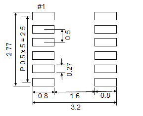
(Unit: mm)
To maintain stable operation, provide a 0.1uF by-pass capacitor
at a location as near as possible to the power source terminal of the crystal product (between Vcc - GND).
