- RTC Top
- What is RTC Modules?
- Epson's RTC Modules
- Features
- Scenes
- RTC Modules for Automotive
- Development Tools
- Videos
RX8804CE :I2C-Bus Interface Real Time Clock Module
(Built-in 32.768 kHz-DTCXO)
- Built in frequency adjusted 32.768 kHz crystal unit and DTCXO.
- Interface Type
I2C-Bus interface (400kHz)
- Interface voltage range
1.6 V to 5.5 V
- Temp. compensated voltage range
1.5 V to 5.5 V
- Clock supply voltage range
1.5 V to 5.5 V
- Selectable clock output(32.768 kHz, 1024 Hz, 1 Hz)
- The various functions full calendar, alarm, timer, event detection
- The time-stamp synchronizing to the event detection of EVIN-pin
- The SOUT-pin outputs that selected flag bit value
Video contents: RX8804CE, RA8804CE SOUT Function
- Applications : handy equipment , outdoor unit , industrial machine
- Epson prepared Linux driver and evaluation board for development
https://www5.epsondevice.com/en/information/support/linux_rtc/The registered trademark Linux® is used pursuant to a sublicensehttps://www5.epsondevice.com/en/information/support/rtc_evaboard/
from LMI(Linux Mark Institute) - Links to Driver and Video contents
Click here


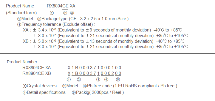
RX8804CE
Design Support Data Download
Block diagram
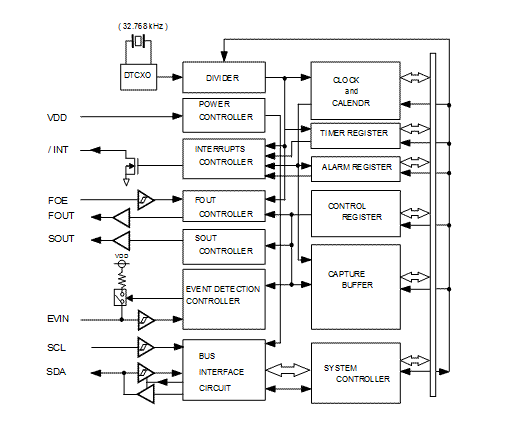
Overview
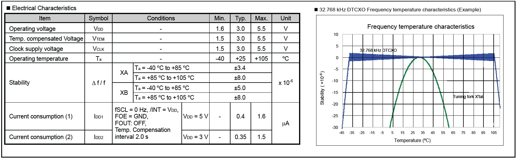
- Stability
- XA
± 3.4 x 10⁻⁶ / -40 °C to +85 °C ( Equivalent to ±9 seconds of month deviation )
± 8.0 x 10⁻⁶ / +85 °C to +105 °C ( Equivalent to ±21 seconds of month deviation ) - XB
± 5.0 x 10⁻⁶ / -40 °C to +85 °C ( Equivalent to ±13 seconds of month deviation )
± 8.0 x 10⁻⁶ / +85 °C to +105 °C ( Equivalent to ±21 seconds of month deviation )
- XA
- 32.768 kHz frequency output function
- FOUT pin output (C-MOS output), CL = 30 pF
- Output selectable: 32.768 kHz, 1024 Hz, 1 Hz
- Event detection function
- when trigger input to EVIN-pin or specified by program, time and date is recorded.
The EVIN-pin with pull-up resistor that is releasable.
- when trigger input to EVIN-pin or specified by program, time and date is recorded.
- Timer function
- Timer source clock are 1min., 1sec., 64Hz, 4096Hz.
- 24-bit-presettable counter (244µs to about 32years(280320h).
- Alarm function
- Alarm function can be set to day of week, day, hour, and minute.
- Internal state output function
- SOUT pin output (C-MOS output).
- it outputs selected flag-bit value or specified value(H or L).
Specifications (characteristics)
Pin function
| Signal Name | I / O | Function |
|---|---|---|
| SOUT | Output | Internal state output pin./td> |
| SCL | Input | Serial clock input pin |
| FOUT | Output | The pin outputs the reference clock signal ( CMOS output ) |
| EVIN | Input | Event input pin |
| VDD | - | Connected to a positive power supply |
| FOE | Input | The input pin for the FOUT output control |
| / INT | Output | Interrupt output (N-ch. open drain) |
| GND | - | Connected to a ground |
| T2 | - | Use only for testing in the factory ( Do not connect externally ) |
| SDA | I/O | Data input and output pin |
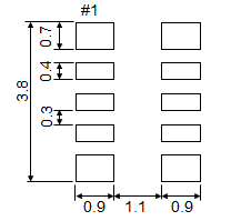
Terminal connection/External dimensions
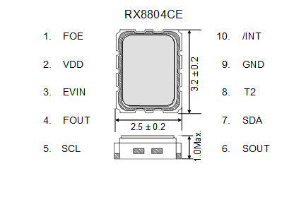
(Unit: mm)
Footprint (Recommended)
(Unit: mm)
To maintain stable operation, provide a 0.1uF by-pass capacitor
at a location as near as possible to the power source terminal of the crystal product (between Vcc - GND).
Links
Video contents: How to use Real Time Clock Module evaluation board(RX8900CE, RX8804CE)
Video contents: RX8111CE: Battery backup switchover function
Video contents: RX8111CE: Time stamp function
Video contents: RX8111CE: Wake up timer function
Video contents: RX4111CE: Battery backup switchover function
Video contents: RX8804CE, RA8804CE SOUT Function
Real Time Clock: RX8900CE / RX8804CE Evaluation Tools
Linux® Driver for Real Time Clock Module
The registered trademark Linux® is used pursuant to a sublicense from LMI (Linux Mark Institute)
