Handling Precautions
Please use the each product under the conditions provided in respective specifications and catalogues. The crystal products are designed and manufactured to satisfy its specification, and quality and reliability of the products are ensured through our stringent reliability tests before shipments. However, it is essential to store, mount, and use the products under proper conditions in order to keep the quality and reliability. Please pay careful attention to following precautions and use the products under the optimal conditions. We shall not be responsible for any deteriorated performance of the products caused by any application or usage of the products adopted at customer's own discretion.
Common points for all products
Crystal Oscillator and real time clock module
Common points for all products
-
Shock resistance.
Crystal products may be damaged under some conditions, such as dropping from desks or receiving shocks during mounting. Please do not use the products if products have received any excessive shocks.
-
Radiation
Exposure to radiation can cause deterioration in performance, so avoid irradiation.
-
Chemicals /pH
Do not use or store the product in a pH range that may cause corrosion or dissolution of the materials or packaging.
-
Adhesive
Do not use an adhesive that may cause corrosion of the packing materials, terminals, components, glass materials, and vapor deposited materials used in the products. (For example, a chlorine-based adhesive may corrode the metal parts "lid" of a crystal unit to diminish the hermetic qualities, lowering the performance.)
-
Halogen Compound
Do not use products in halogen gas. Even a slight amount of halogen gas, such as that found in chlorine gas in the air or in metal parts used in the package, may corrode. Also, do not use any resin that emits halogen gas.
-
Static electricity
Excessive levels of static electricity may damage the product, please treat it in anti-static condition. Choose conductive materials for containers and packing materials. Use a soldering gun and a measurement circuit free from high-voltage leakage and provide grounding conduction when working with them.
-
When designing
7-1:The affect of mechanical vibration
While there is any given shock or mechanical vibration periodically to crystal products, such as, a piezo sounder, a piezo buzzer, and speaker, to crystal products, output frequency and amplitude can be changed. Especially the quality of telecommunication equipment could be affected by this phenomenon. Although Epson's crystal products are designed to minimize the effect of mechanical vibration, we recommends to check them in advance and to follow the PCB design guidelines as below.
7-2:PCB design guidelines
(1) Ideally, the mechanical buzzer source should be mounted on a separate PCB from the crystal device. It is advisable to use cushion or cutting PCB, if you mount on same PCB. Traveling mechanical vibration differs when applied to the PCB only vs. inside the body. It is advisable to confirm characteristics in the body.
-
(2) Refer Epson's recommend footprint when designing.
(3) In case of using solder flux, please use it on the basis of the flux of the JIS standard (JIS C 60068-2-20/IEC 60,068-2-20).
(4) Please use the solder on the basis of the JIS standard (JIS Z 3282, Pb content 1000ppm, 0.1wt% or less) lead -free solder.
-
Notes on storage
(1) Storing the crystal products under higher or lower temperature or high humidity for a long period may affect frequency stability or solderability. Please store the crystal products at the normal temperature and humidity, avoid storing them for a long period and mount them as soon as possible after unpacking.
Normal temperature and humidity:
Temp,+15°C to+35°C, humidity 25 % RH to 85 % RH(refer to the standard conditions of test site JIS C 60068-1/IEC 60068-1)(2) Please carefully handle the inner and outer boxes and reel. External pressure may cause deformation of reel and tape.
-
Mounting precautions
9.1 Soldering heat resistance
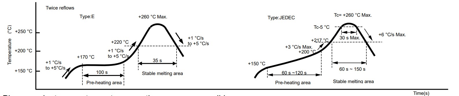
The crystal products except SMD products use solder having a +180°C to +200°C melting point. Heating up the package more than +150°C may deteriorate the characteristics or damage the products. If the crystal products need to be soldered at temperature of more than +150°C, SMD products are recommended. Using higher temperatures over the following reflow conditions to crystal products, even SMD products, may cause the characteristics to deteriorate. The reflow conditions within following profile are recommended. Always check the soldering temperature and time before mounting these products. Also, please check them again when the mounting conditions are changed. Please contact us for inquiries about heat-resistance if crystal products need to be soldered over the following profile.
- (1) SMD products Reflow profile (example)
The availability of the heat resistance for reflow conditions of JEDEC-STD-020D.01 is judged individually. Please inquire it.
Please make temperature rate as gentle a curve as possible.
9.2 Shocks by auto mounting
Shocks caused by auto mounting and vacuuming may deteriorate the characteristics and affect the products. Please set the mounting conditions to minimize the shocks as much as possible, and be sure that there is no affect on the characteristics before mounting. Please review the conditions after the conditions are changed. Also please be sure that crystal products don't hit machines or other electric boards, etc. before or after mounting.
9.3 Notes for each package type
-
(1) Ceramic package products and SON products
Bending the board after soldering ceramic package products and SON products (MC-146,RTC-****NB,RX-****NB) may cause peeling off portions of soldering or package cracks by mechanical stress. Particularly, in the case of cutting boards after soldering these products, please be sure to layout the crystal on a less stressed location and use less stressed cutting method.
-
(2) Ceramic package products
In the case of soldering ceramic package products on a different expansion-coefficient board (ex. Epoxy Glass), soldering crack at the foot pattern would be expected under repeated temperature changes for a long period. Under these conditions, be sure to check the solderability in advance.
-
(3) Cylinder products
Bending the lead on the glass or pulling the lead strongly may cause cracking of the hermetic seal glass at the root of the lead and may cause the air tightness and the characteristics to deteriorate. When the lead of crystal products need to be bent as in the figure below, leave more than 0.5 mm of lead from the case and hold the lead to prevent the lead from cracks. When the lead needs to be repaired, do not pull it, and hold the bent part to correct it. Giving undue pressure on this portion of hermetic seal may cause the air tightness to deteriorate. Please avoid applying pressure. Gluing the case of products on the electric board is recommended to prevent the air tightness from deteriorating.
-
(4) DIP products
Deformed leads cannot be inserted into board holes. Avoid applying stress sufficient to deform leads.
-
(5) SOJ Products and SOP products
Please avoid applying stress sufficient to deform the leads. Deformed leads may cause incorrect soldering. Particularly SOP products need to be handled with the greatest care.
9.4 Ultrasonic cleaning
(1) Products using AT-cut crystal and SAW resonator/filter can be cleaned by ultrasonic methods. But under some conditions, the crystal characteristics may be affected and internal wiring may be damaged. Please be sure to check the suitability of your system in advance.
(2) Products using tuning-fork crystals and gyro sensors cannot be guaranteed if cleaned using ultrasonic methods, because crystal may be destroyed.
(3) Do not wash open-type products.
(4) With washable products, avoid the use of cleaners or solvents that may negatively affect the product.
(5) By solder flux residual moisture absorption and solidification, it may course of migration etc. So, it may affect the reliability and quality of the product negatively. Please clean up the residue of flux and dry the PCB.
- (1) SMD products Reflow profile (example)
-
Handling
Do not touch the surface of IC directly with tweezers or any hard tools, jigs.
-
Use environment (temperature and humidity)
Please use the products within rating temperature range in concern temperature distribution in body and seasonal changes. In high humidity environment, it may cause malfunction caused by the dew condensation. Please prevent dew condensation.
Crystal unit
-
Drive level
Applying excessive drive level to the crystal units may cause deterioration of characteristics or damage. Circuit design must be such as to maintain a proper drive level.
Refer to page "Drive level" -
Negative resistance
Unless adequate negative resistance is allocated in the oscillation circuit, oscillation or oscillation start up time may increase.
Refer to "Allowance for Oscillation". -
Load capacitance
Differences in the load capacitance in the oscillation circuit may result in deviations in the oscillation frequency from the desired frequency. Attempting to tune by force may merely cause abnormal oscillation. Before use, please specify the load capacitance of the oscillation circuit.
Refer to "Load capacitance"
Crystal Oscillator and real time clock module
All crystal oscillators and real time clock modules are provided with an IC.
-
Noise
Applying excessive level of extraneous noise to power source or input terminal may cause latch up or spurious phenomenon,which results in malfunction and breakdown.
-
Power supply line
Line impedance of a power supply should be as low as possible.
-
Output load
It is recommended that output load is installed as close as possible to an oscillator (within 20 mm).
-
Treatment of unused input terminals
Unused pins that are left open may collect noise, thereby resulting in malfunction. Also, power consumption may increase when both P-channel and N-channel are turned on, therefore connect unused input terminals to VCC or GND.
-
Heat impact
Repeated large changes in temperature may degrade the characteristics of a deteriorated crystal unit and cause breakage of wires inside the plastic mold. This must be avoided.
-
Mounting direction
Incorrect mounting of the oscillator may cause malfunction and breakdown, so please check the mounting direction when Installing.
-
Power on
It is not recommend to power on from intermediate electric potential and / or extreme fast power on. Powering on under such conditions may cause no oscillation and / or malfunction.
Sensing device
-
Interference between the sensors
The crystal sensor may catch the interference by board vibration and power supply common impedance.
-
Protection against vibration
Please consider about protection against vibration when the crystal sensor is operated in vibration condition.
