About QMEMS

Electric device market needs
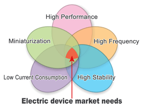
Electric device performance typically deteriorates with miniaturization. The market needs electric devices that offer the same high performance even after they are downsized.
Epson's competitive advantage lies in QMEMS, crystal devices that meet these market requirements.
*QMEMS and its logos are registered trademarks or trademarks of Seiko Epson Corporation in Japan and other countries.
What is QMEMS?
QMEMS is a combination of 'Quartz', a crystal material with excellent characteristics such as high stability and high precision, and "MEMS" (a microfabrication technology). To a semiconductor MEMS material, we apply precision microprocessing based on quartz material to create a quartz device that we call 'QMEMS' which offers high performance in a compact package.

The QMEMS lineup
Applying our photolithography processing technology, proven in over 30 years of tuning-fork crystal unit production, we provide a range of subminiature, high-precision, high stability quartz devices.
Timing devices

Miniaturizing tuning-fork crystal units results in a greater CI value (the criteria for oscillation loss in crystal), and obtaining satisfactory oscillation characteristics imposed a limit on miniaturization. Using photolithography, Epson has overcome this limitation to achieve a subminiature product.

In order to increase the frequency of oscillators, it is necessary to make the chip thinner, but conventional processing methods imposed limitations on producing thin chips.
Using photolithography, Epson overcame this limitation by making only the part close to the excitation electrode thinner (reverse-mesa structure), thus maintaining the strength of the chip. In this way we achieved basic oscillation at high frequency bands of 100 MHz and above.

In producing miniature crystal chips, increased variability in characteristics represents an obstacle, leading to a reduction in mass production efficiency.
Using photolithography on each wafer, Epson has improved process precision to achieve ultra compact quartz chips with uniform characteristics. This has enabled substantial increases in mass production efficiency in the field of subminiature devices.
Sensing devices

Applying the tuning-fork crystal unit chip structure. Using our photolithography processing technology to the full, Epson has achieved ultra compact devices of 2 × 2 mm.
We have created compact yet highly sensitive gyro sensors using a hammerhead and H-groove structure produced with photolithography.
