Part2. Photolithography opens up the future
February.2012

Time passes by all too quickly. It had been 5 years since the quartz watch that astounded the world, the ‘Seiko Quartz Astron 35SQ,’ had been brought to market. The quartz watch had already become an indispensable tool in people's daily lives, and had become widely popularized. However, awaiting the top manufacturer at that time, Suwa Seikosha Co., Ltd., was a difficult period of stiff competition from rival companies. It had been crucial that the company continue making quartz watches even more compact and affordable, in order to maintain the dominant position it had held until then. However, tuning fork crystal units, the very heart and soul of these watches, were already as small and cheap as technological limitations would allow. How could they overcome the impending crisis? The solution they eventually chose was the implementation of a completely unknown technology. This second installment of ‘The QMEMS Story’ will explore the efforts of the engineers involved in the technological development of QMEMS' origins.
On the surface, everything seemed to be going smoothly. However…
The year 1974 marked the fifth year since the birth of the world's first quartz watch, the ‘Seiko Quartz Astron 35SQ.’ It was at this time that quartz watches became fully popularized, and production of tuning fork crystal units had to be increased constantly in order to keep up with demand. It was the Quartz Device Division (then Matsushima Industry Co., Ltd.) in Ina, Nagano Prefecture, that was tasked with overseeing the volume production of these devices (see Figure 1). With production and other factors proceeding so smoothly, it seemed as though they could confidently rely on tuning fork crystal units to maintain their core business. Everyone working at the Ina plant was steeped in a deep sense of satisfaction.
On the surface, everything seemed to be going smoothly. However, the engineers working at the forefront of development had no time to rest. Heated arguments were beginning to take place on a daily basis between the engineers at Suwa's Watch Design Division and those at Ina Quartz Device Division. For watch manufacturers, the ability to make devices smaller and more affordable was vital, and they barely had time to pause for breath.
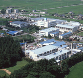
Figure 1: The Crystal Device Division located in Ina, Nagano Prefecture.
An aerial view overlooking Seiko Epson's Ina plant in the 1990s. The large, flat structure behind the 3-storey building was constructed for the expansion of photo processes.
The Quartz Device Division understood the wishes of the Watch Design Division. But it was simply not possible to make tuning fork crystal units any smaller than they already were. The Watch Design Division, on the other hand, needed the crystal units to be made more compact so that they could move on to their next commercial product line of ladies' watches. They were desperate for the engineers to come up with something.
There was a reason behind the Suwa Watch Design Division's stubborn refusal to back down. It had been 5 years since they had first launched the world's first quartz watch, and competition in the market was becoming increasingly tough, particularly with Hong Kong's sudden rise in manufacturing. It was therefore essential to continue making watches more compact and affordable in order for the company to maintain its dominant position. Accordingly, they began to consider bringing to market a new line of ladies' watches that would be dramatically smaller than existing watches. To achieve this, it was absolutely crucial that they be able to make tuning fork crystal units ? the very heart of these devices - yet smaller again.
However, nothing is without its limitations. ‘Of course, it was possible in theory to make these crystal units even smaller. But that would have caused costs to skyrocket. So the fact remained that in practice, it wasn't really possible to make them any smaller after all.’ This was the true position of the Quartz Device Division. As usual, the inter-divisional arguments were going nowhere.
‘Suwa men and Ina women’
The engineers at the Quartz Device Division understood only too well the painful predicament faced by the Watch Design Division. Although they fervently wished they could help them, there wasn't really much they could do because manufacturing processes for tuning fork crystal units had already reached technological limitations.
Let us pause to review a simple explanation of what was covered by the manufacturing process in 1974. Firstly, a tuning fork (U-shaped) quartz fragment was mechanically cut out of a quartz wafer. This method meant that there was a great deal of variation at this stage between the lengths of the left and right ‘arms’ of the U-shaped fragment, making it hard to ensure a balance between the two arms. This variation could be 10µm or more. To remedy this, workers corrected the arm lengths of each individual quartz fragment using a diamond wheel, thus improving the precision to 20ppm. This task was extremely complicated and required much patience. It was at this point that tasks relying on human craftsmanship were reaching their limits.
This kind of laborious task was made possible through the efforts of the female workers, who were adept at performing the intricate procedures required (Figure 2). There is a saying in Nagano Prefecture, that "Ina women are well-suited to Suwa men." The gentle, patient personalities of Ina women are said to combine perfectly with the gallant nature of men from Suwa, creating the perfect couple. It was the fervent efforts of these ‘Ina women’ that had helped the company to survive thus far.
However, the effects of variation gradually began to become more noticeable as tuning fork crystal units were frequently made ever more compact. As the required adjustments became even more detailed than ever before, the time needed to perform adjustments on each tuning fork crystal unit also grew longer. Naturally, it was still a comparatively short process for the already well-experienced Ina women, but training and nurturing this type of worker was not an easy task. It goes without saying that if more time had to be spent on manufacturing, costs would also escalate. So far, the company had managed to curb any problems thanks to the efforts of these ‘Ina women,’ but they could no longer rely on this alone as the full-fledged popularization of quartz watches was beginning in earnest.
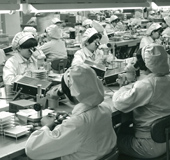
Figure 2: Frequency adjustment process for tuning fork crystal units
Frequency adjustment process for tuning fork crystal units in the early 1970s. This image shows the women at work using a diamond wheel to hand-cut the front edge of tuning fork crystal units, in order to adjust the frequency.
Amidst the uneasy feeling of not knowing whether they would be able to cope, they held out hope for finding a clever way to resolve the problem.
That morning in the meeting room, they began to search for a manufacturing method that would enable them to simultaneously produce smaller and cheaper devices, but a heated exchange ensued. Then one of the engineers spoke up. ‘Don't you think we're nearly ready to begin using that other technology…?’
Development begins on the ‘voice of authority’
‘That other technology’ was a reference to ‘photolithography,’ a technology that the Research & Development Division had been concentrating their development on since around 1970. Photolithography is a technology that creates microscopic patterns by applying photographic exposure techniques. At the time, photolithography had already become an indispensable manufacturing technology for integrated circuits (ICs).
A U.S. firm named Statek Corporation was the first in the world to succeed in applying photolithography technology in the manufacturing of crystal units. Upon hearing this news, Ichiro Hattori (then a company director of Suwa Seiko) flew immediately to the U.S. Whilst there, he was briefed on the implementation of this technology and when he returned to Japan, he promptly ordered the Research & Development Division to work on putting this technological development into practice.
Theoretically, application of photolithography technology to the processing of crystal units should facilitate dramatic improvements in process accuracy. However, even if they succeeded in using this technology in thin-film processing on silicon wafers, they were concerned whether they would be able to apply it to the quartz wafers themselves. And even if that could be achieved, they did not know whether they would be able to obtain the results they were truly after. The truth is that there were many engineers who felt doubtful of this.
Still, it was clear that they would soon reach their limits if they continued with mechanical processing methods. Furthermore, according to Haruo Takada, ‘The corporate ethos of Suwa Seiko at that time was to boldly take on new challenges.’ So they established a Project Team and began their development of photolithography technology use in tuning fork crystal units. The new Project Team moved quickly. They had documentation sent over from the U.S. and began to conduct basic experiments implementing a photolithographic prototype installation.
The photolithography technology was truly amazing (Figure 3). The engineers were astounded by the incredible potential they could see as soon as they began their basic experiments. Quartz device engineer Mutsumi Negita says that "Even at the basic experimentation stage, we could see that our process accuracy was at least 10 times better than our mechanical methods." It seemed that photolithography technology would be a very worthwhile successor technology to their processing methods.
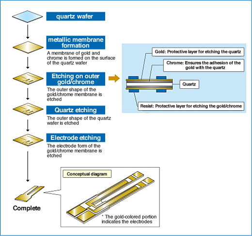
Figure 3: The process flow of photolithography technology at that time
A photographic exposure technique is used to extract a quartz fragment in the desired shape from the quartz wafer, and to form electrodes in microscopic patterns.
Still, the new technology was not without its limitations. Statek's original device design was not well-suited to obtaining high performance from tuning fork crystal units. The low electric field efficiency meant that the crystal impedance (CI value)*1 was extremely high. When the CI value is high, it can be difficult to oscillate the crystal unit, and the design of the oscillating circuit also becomes more complicated. ‘Although the high process accuracy was superb, the technology could not be used in its present state.’ This was the impression of the engineers working at the Ina Quartz Device Division upon assessing the first prototypes.
Although there was no doubt that the technology had great potential for the future, they were unable to use it straight away. With this in mind, they decided they had to go back to the drawing board to conduct further research and development in photolithography.
*1 Crystal impedance refers to the equivalence series resistance of a crystal unit. Generally speaking, a crystal unit is oscillated using an electrical circuit that combines a condenser with resistance. When the crystal impedance (CI value) is high, it becomes difficult to oscillate the crystal unit.
A new breakthrough emerges from their own unique technology
For just over the next 2 years, they worked on a huge breakthrough in photolithography technology: the development of a new electrode structure for tuning fork crystal units*2.
The original electrode structure developed by Statek was only able to obtain electric field efficiency of around 30%, and the CI value was too high. So the Project Team decided to modify the cut angle*3 of the quartz material and formulate an optimal structure to suit it. As a result, they succeeded in dramatically increasing the electric field efficiency. In the meantime, although the CI value was still high in comparison to tuning fork crystal units manufactured using mechanical processing methods, it had fallen to a figure that was low enough to be usable. ‘With levels like these, we should be able to come up with something.’ This had been the reason behind the engineer's previous comment in the meeting room, about ‘being nearly ready to use that other technology…’
The issue with photolithography technology had been that CI values were too high. However, the full spectrum of benefits offered by high process accuracy would become accessible only if this hurdle could be cleared. Many engineers felt the same way. The decision that day in the meeting room to implement photolithography technology had been unanimous.
With the biggest issue of all now resolved, they were once again amazed by the potential being uncovered by photolithography technology. Process accuracy of more than 10 times the levels of mechanical methods gave rise to various beneficial ripple effects. One of these was the mount method for quartz fragments. The variation in measurements between the left and right arms of the U-shaped fragments that had occurred with conventional mechanical processing methods generated a component known as oscillation leakage. Degradation of properties would occur when this leakage escaped externally. To combat this, a complicated mount structure was adopted using a spring, to help prevent this degradation via oscillation leakage. However, with the increased process accuracy brought by the implementation of photolithography technology, and the reduced variation between measurements of the left and right arms, the spring was no longer needed. It had become possible to simply attach the quartz fragment directly to the lead terminal for the airtight seal. This contributed greatly to reduced costs and to making the size much more compact.
Another beneficial ripple effect was the method used to adjust the frequency. Previously, each individual fragment had to be adjusted by a worker using a diamond wheel. This required a vast number of labor hours. However, now that process accuracy had been so greatly improved thanks to the implementation of photolithography technology, no more than a fine tune would be needed. Now, this could be achieved simply by adopting a method to trim the membrane with a laser, which would also automate the fine-tuning process. The result was that productivity could be streamlined dramatically.
*2 This technological development earned them Japan Patent Office Director-General Award of the 1982 National Commendation for Invention. The recipients were the 4 members of the Project Team who had fulfilled the most central roles, namely Kikuo Oguchi?, Akio Shimoi, Makoto Shibata and Toshiaki Ogata.
*3 The crystalline structure of artificial quartz is trigonal. Accordingly, the properties will be different according to the angle at which each thin quartz wafer is cut out.
Clouds always follow the sunshine…
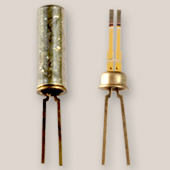
Figure 4: The first product manufactured using photolithography technology.
The ‘C-002’ was first commercialized in 1975. Its external dimensions were 2mm (radius) x 6mm (length), with normal frequency of 32.768kHz.
Meanwhile, another new technology was being quietly developed to support the implementation of photolithography technology. The company's preparation was watertight. And at last, volume production of ‘C-002,’ the first tuning fork crystal unit to have photolithography technology applied, began in 1975 (Figure 4). Its external dimensions were 2mm (radius) x 6mm (length). It was tiny at just 1/7 the size of the previous generation of crystal unit, ‘Type Cal.57’ (Figure 5). They had succeeded spectacularly in making crystal units more compact.
As for costs, these should also have been drastically reduced thanks to the streamlined structure and innovation of the manufacturing process. But clouds always follow the sunshine. There was one problem in particular that was troubling them on the manufacturing floor. Their fabrication yield was extremely low. According to Mutsumi Negita, the Project Team member in charge of the technological development for volume production using photolithography at that time, ‘The fabrication yield when we began volume production was around 10%.’ In other words, around 9 products out of every 10 produced were defective. However, we needed to produce 50,000 crystal units per month now that the product had been brought to market. ‘All our workers forewent their vacation time in order to somehow be able to produce 50,000 good products per month.’
They felt that they might be able to cope with this ‘emergency response’ schedule if it only lasted around a month, but it would not be sustainable long-term. One by one, the workers in the Quartz Device Division succumbed to exhaustion. Upon observing this situation, others within the company began to wonder whether using this new technology was truly going to be achievable at low costs, and whether they had in fact been better off previously, when they had still used mechanical process methods. The engineers in the Quartz Device Division themselves began to wonder whether in fact their judgment had been correct.
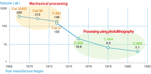
Figure 5: Timeline indicating how tuning fork crystal units have become more compact
The implementation of photolithography technology enabled a huge reduction in size. Although not mentioned in this article, other products were also brought to market following the ‘C-002,’ including the ‘C-004’ in 1978 [dimensions 1.5mm (radius) x 5mm (length)], and the ‘C-005’ in 1981 [dimensions 1.2mm (radius) x 4.6mm (length).]
Woodworking hints at a solution to the problem
They had to find a way to get themselves out of this predicament. A new Project Team was organized to improve the fabrication yield, headed by the engineer in charge of production technology. A young engineer by the name of Mutsumi Negita was included in the Team.
The Project Team's first assignment was to find the cause of the lowered yield. They used a microscope to examine the surface of defective tuning fork crystal units, and were amazed to reveal the presence of an immeasurable number of pinholes. These were being caused during the etching process of the quartz material. After several weeks of investigating the unknown cause of the pinholes, they were able to discover a fine covering of dirt that was attached to the quartz wafers. If etching was performed on the membrane which had been inadvertently formed on top of this dirt, it would cause poorer adhesion over the dirty portion, resulting in pinholes.
They therefore attempted to thoroughly remove this dirt, by reviewing their handling of the quartz wafers and tweaking their cleaning methods. Success! They were able to remove sufficient dirt, and everyone on the Yield Improvement Project Team felt a wave of relief.
Anticipating wonderful results, they were nevertheless surprised and disappointed to learn from the manufacturing floor that in fact, the yield rate had barely improved at all. It seemed that simply removing the dirt was not enough to produce the desired results. So their solution had been short-lived ? perhaps they still hadn't found the true cause of the original problem…? Once again, they examined the surface of the defect crystal units under the microscope. The pinholes were still there! ? But why? This time, they had no idea at all what the root of the problem could be. The Yield Improvement Project Team investigated a variety of different possibilities, everything they could think of. However, the yield rate did not budge, and time passed by in vain.
Then, a curious thing occurred to Mr. Negita one day, as he was at home absorbed in his hobby of woodworking. In woodworking, polishing powder is applied to the rough surface of boards prior to coating with another substance such as varnish. This gives the surface of the final product a much better finish. This concept gave him a flash of inspiration. ‘Perhaps the surface of the quartz wafer is also rough, like this wood…’ It was certainly a possibility. Quartz wafers are mechanically cut out from large pieces of artificial quartz before being polished (Figure 6). It was entirely conceivable that the surface layer could become roughened from the stress of this process.
So Mr. Negita decided to try removing the entire surface layer of the quartz wafer by etching, and then forming a membrane on the top. It worked! Not a single pinhole was formed! Previously, the process had involved forming a membrane on the top of the roughened surface layer, and this had resulted in the many pinholes.
The yield rate skyrocketed immediately. They were finally able to secure a sufficient supply of good products without having to work on their days off. Furthermore, the negative impression of photolithography technology that had been smoldering within the company was dispelled as soon as the yield rate escalated.
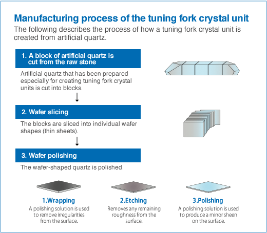
Figure 6: Artificial quartz and quartz wafers
Thin quartz wafers are manufactured by mechanically slicing pieces of artificial quartz made using a specialist device known as an autoclave.
The final hurdle behind them, they moved on to the beginnings of QMEMS
Their devices had now reached 1/7 the size of conventional tuning fork crystal units, with greatly reduced manufacturing costs. ‘It would be a waste to confine such a groundbreaking device to our company alone. We must sell it externally so that many more watch manufacturers can take advantage of our technology.’ With the call to share the technology growing within the company, external sales of the ‘C-002’ began in 1976.
They felt sure that their new crystal units would create a real stir within the market and that they would be flooded with inquiries from customers around the globe. The Ina Quartz Device Division waited excitedly in anticipation. They distributed sample products with the dimensions 2mm (radius) x 6mm (length), and the response to the new shape was extremely favorable. However, they found that very few companies actually adopted their new technology, with the reason being that it was difficult to use.
Until then, many customers had used large-sized tuning fork crystal units that had been manufactured using mechanical process methods. In comparison, the ‘C-002’ was much harder to oscillate. Although the company had kept the CI value as low as possible, it was still quite high compared to conventional tuning fork crystal units. Although the company's own Watch Design Division had highly praised the more compact external dimensions and had adopted these new crystal units, other watch manufacturers were reluctant to use them, citing their difficulty of use.
They already knew why CI values became higher. Photolithography technology uses light to form electrode patterns, so while it was possible to process the top surface of the crystal units, the same was not possible for the sides as they were not exposed to the light. Electrode patterns could not be created on the sides of the crystal units, resulting in a higher CI value.
They would need to establish a technology for three-dimensional photolithography in order to form electrodes on the sides of the devices as well. This was a technology that had not yet been put into practice by even the IC industry, who were the leaders in implementation of photolithography technology. It was Mr. Negita that was placed in charge of the development of this new technology. "At first, we had to devise a provisional method for creating electrodes on the sides of crystal units, so as to achieve a product that customers could use, and we began volume production accordingly. Furthermore, in parallel to this, we spent over a year developing a permanent method that would connect us to this objective in a lasting manner, and we succeeded. Our provisional method had been plagued by the dual problems of yield and working efficiency, and our Manufacturing Division was constantly berating us for it" says Mr. Negita, reflecting on the situation at that time.
So what is this three-dimensional photolithography technology? Unfortunately, we are unable to explain the details within the scope of this article, as this is the same technology that currently supports the framework of Epson Toyocom. The ‘technology to manufacture tuning fork crystal units using photolithography technology’ was developed in Ina, Nagano Prefecture, some 36 years ago. And this is the origin of ‘QMEMS.’
By Technical Writer, Katsumi Yamashita
(To be continued)
interview
 |
Joined Suwa Seikosha Co., Ltd. in 1963. For approximately 28 years, from around 1972 until his retirement in 2000, Mr. Takada was involved in the development of quartz devices. Born and raised in Shinjuku, Tokyo, Mr. Takada cites his ‘unparalleled love of trains’ as his reason for becoming an employee of Suwa Seikosha. ‘At the time, the main Chuo [train] Line linking Kofu to the Kami-Suwa region had just been electrified. I wanted to ride the trains on that line more than anything, so I relinquished a job offer with an aircraft manufacturer that was almost finalized, and chose Suwa Seikosha in Nagano instead.’ |
 |
Joined Matsushima Industry Co., Ltd., a subsidiary of Suwa Seikosha Co., Ltd. (now known as Seiko Epson Ina Plant) in 1974. Mr. Negita became engaged in the development of quartz devices immediately thereafter, and has continued in this vein for the 37 years ever since. Mr. Negita is currently (as at September, 2011) an instructor for the next generation group of engineers in his role as the Deputy Chief of the TD Production Engineering Department. |
QMEMS is a registered trademark of Seiko Epson Corporation.
