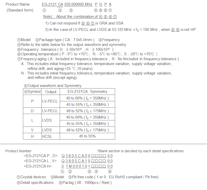
EG-2121CA (Crystal Oscillator Low-Jitter SAW Oscillator)
- Frequency range
53.125MHz to 700MHz - Supply voltage
2.5V Typ. - Output
LV-PECL or LVDS or HCSL - Function
Output enable (OE) - External dimensions
7.0 × 5.0 × 1.2mm - Very low jitter and low phase noise by SAW unit.
![]()
![]()

EG-2121CA
Specifications
LV-PECL Output
| Item | Symbol | LV-PECL | Conditions/Remarks | |
|---|---|---|---|---|
| Output frequency range | f0 | 53.125MHz to 500MHz | Please contact us for inquiries regarding available frequencies. | |
| Supply voltage | VCC | 2.5V ± 0.125V | ||
| Storage temperature | T_stg | -40°C to +100°C | Store as bare product. | |
| Operating temperature | T_use | P : 0°C to +70°C R : -5°C to +85°C S : -20°C to +70°C |
||
| Frequency tolerance | f_tol | G : ± 50 × 10-6 H : ±100 × 10-6 |
||
| Current consumption | ICC | 80mA Max. | OE = VCC , L_ECL = 50Ω | |
| Disable current | I_dis | 20mA Max. | OE = GND | |
| Symmetry | SYM | P : 40% to 60% ( f0 > 350MHz ) |
at outputs crossing point | |
| P : 45% to 55% ( f0 ≦ 350MHz ) |
||||
| D : 48% to 52% ( f0 ≦ 175MHz ) |
||||
| Output voltage | VOH | 1.55V Typ. | DC characteristics | |
| VCC - 1.025V to VCC - 0.88V | ||||
| VOL | 0.8V Typ. | |||
| VCC - 1.81V to VCC - 1.62V | ||||
| Output load condition (ECL) |
L_ECL | 50Ω | Terminated to VCC - 2.0V | |
| Input voltage | VIH | 70% VCC Min. | OE terminal | |
| VIL | 30% VCC Max. | |||
| Rise time / Fall time | tr / tf | 400ps Max. | Between 20% and 80% of ( VOH - VOL) | |
| Start-up time | t_str | 10ms Max. | Time at minimum supply voltage to be 0s | |
| Phase Jitter | tPJ | 0.8ps Max. | f0 < 100MHz | Offset frequency: 12kHz to 20MHz |
| 0.5ps Max. | 100MHz ≦ f0 < 200MHz | |||
| 0.3ps Max. | 200MHz ≦ f0 | |||
| Frequency aging | f_aging | ± 10 × 10-6 / year Max. | +25°C , First year , VCC = 2.5V | |
LVDS Output
| Item | Symbol | LVDS | Conditions/Remarks | |
|---|---|---|---|---|
| Output frequency range | f0 | 53.125MHz to 700MHz | Please contact us for inquiries regarding available frequencies. | |
| Supply voltage | VCC | 2.5V ± 0.125V | ||
| Storage temperature | T_stg | -40°C to +100°C | Store as bare product. | |
| Operating temperature | T_use | P : 0°C to +70°C R : -5°C to +85°C S : -20°C to +70°C |
||
| Frequency tolerance | f_tol | G : ± 50 × 10-6 H : ±100 × 10-6 |
||
| Current consumption | ICC | 30mA Max. | OE = VCC , L_LVDS = 100Ω | |
| Disable current | I_dis | 20mA Max. | OE = GND | |
| Symmetry | SYM | L : 40% to 60% ( f0 > 350MHz ) |
at outputs crossing point | |
| L : 45% to 55% ( f0 ≦ 350MHz ) |
||||
| V : 48% to 52% ( f0 ≦ 175MHz ) |
||||
| Output voltage | VOD | 350mV Typ. 247mV to 454mV |
VOD1 , VOD2 | DC characteristics |
| dVOD | 50mV Max. | dVOD = | VOD1 - VOD2 | | ||
| VOS | 1.25V Typ. 1.125V to 1.375V |
VOS1 , VOS2 | ||
| dVOS | 150mV Max. | dVOS = | VOS1 - VOS2 | | ||
| Output load condition (LVDS) |
L_LVDS | 100Ω | Connected between OUT to OUT | |
| Input voltage | VIH | 70% VCC Min. | OE terminal | |
| VIL | 30% VCC Max. | |||
| Rise time / Fall time | tr / tf | 400ps Max. | Between 20% and 80% of Differential Output peek to peek voltage | |
| Start-up time | t_str | 10ms Max. | Time at minimum supply voltage to be 0s | |
| Phase Jitter | tPJ | 0.8ps Max. | f0 < 100MHz | Offset frequency: 12kHz to 20MHz |
| 0.5ps Max. | 100MHz ≦ f0 < 200MHz | |||
| 0.3ps Max. | 200MHz ≦ f0 | |||
| Frequency aging | f_aging | ± 10 × 10-6 / year Max. | +25°C , First year , VCC = 2.5V | |
HCSL Output
| Item | Symbol | HCSL | Conditions/Remarks | |
|---|---|---|---|---|
| Output frequency range | f0 | 100MHz to 350MHz | Please contact us for inquiries regarding available frequencies. | |
| Supply voltage | VCC | 2.5V ± 0.125V | ||
| Storage temperature | T_stg | -40°C to +125°C | Store as bare product. | |
| Operating temperature | T_use | P : 0°C to +70°C , R : -5°C to +85°C , S : -20°C to +70°C |
||
| Frequency tolerance | f_tol | G : ± 50 × 10-6 H : ±100 × 10-6 |
||
| Current consumption | ICC | 80mA Max. | OE = VCC , L_HCSL = 50Ω | |
| Disable current | I_dis | 20mA Max. | OE = GND | |
| Symmetry | SYM | 45% to 55% | at outputs crossing point | |
| Output voltage | VOH | 0.75V Typ. | DC characteristics | |
| VOL | -0.3V Typ. | |||
| Output load condition (HCSL) |
L_HCSL | 50Ω | Terminated to GND | |
| Input voltage | VIH | 70% VCC Min. | OE terminal | |
| VIL | 30% VCC Max. | |||
| Rise time / Fall time | tr / tf | 500ps Max. | Between 0.175V and 0.525V of output | |
| Start-up time | t_str | 10ms Max. | Time at minimum supply voltage to be 0s | |
| Phase Jitter | tPJ | 0.8ps Max. | f0 < 100MHz | Offset frequency: 12kHz to 20MHz |
| 0.5ps Max. | 100MHz ≦ f0 < 200MHz | |||
| 0.3ps Max. | 200MHz ≦ f0 | |||
| Frequency aging | f_aging | ± 10 × 10-6 / year Max. | +25°C , First year , VCC = 2.5V | |
Jitter
| Item | Symbol | Specifications | Remarks |
|---|---|---|---|
| Jitter * | tDJ | 0.2ps Typ. | Deterministic Jitter |
| tRJ | 3ps Typ. | Random Jitter | |
| tRMS | 3ps Typ. | σ (RMS of total distribution) | |
| tp-p | 25ps Typ. | Peak to Peak | |
| tacc | 4ps Typ. | Accumulated Jitter(σ) n=2 to 50000cycles |
* Based on DTS-2075 Digital timing system made from WAVECREST with jitter analysis software VISI6. : Differential LV-PECL, LVDS output
* Based on SIA-3100C signal integrity analyzer made from WAVECREST. : HCSL output
External dimensions
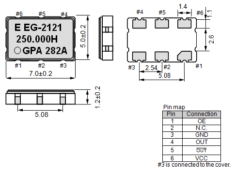
(Unit: mm)
OE pin = HIGH : Specified frequency output.
OE pin = LOW : Output is high impedance
Footprint (Recommended)
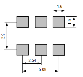
(Unit: mm)
To maintain stable operation, provide a 0.01uF to 0.1uF by-pass capacitor at a location as near as possible to the power source terminal of the crystal product (between Vcc - GND).
