SG-8506CA I2C-Bus Programmable Crystal Oscillator (SPXO) Output LV-PECL
- Frequency range50MHz ~ 800MHz
- Supply voltage2.5V to 3.3V
- External dimensions7.0 × 5.0 × 1.5mm (8pins)
- Features
Programmable frequency by 7-bit I2C slave addressHigh frequency fundamental tone crystalLow jitter PLL technology
- ApplicationOTN, BTS, Test Instrument
![]()
![]()

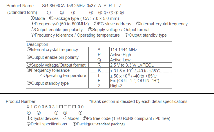
SG-8506CA
Design Support Data Download
Specifications (characteristics)
| Item | Symbol | Specifications | Remarks |
|---|---|---|---|
| Output frequency range | f0 | 50MHz to 800MHz | It can be changed by I2C |
| Supply voltage | VCC | 2.5V-0.125V to 3.3V +0.33V | - |
| Storage temperature | T_stg | -55°C to +125°C | Store as bare product after packing |
| Operating temperature | T_use | -40°C to +85°C | - |
| Frequency tolerance*1 |
f_tol | ±31.5 × 10⁻⁶ | Customized Product (Option) |
| ±50 × 10-6 | |||
| Current consumption | ICC | 90mA Max. | OE Active, L_ECL=50 Ω |
| Disable current | I_dis | 40mA Max. | OE Inactive, Output Standby: Hi-Z mode |
| 70mA Max. | OE Inactive, Output Standby: Fix mode | ||
| Symmetry | SYM | 45% to 55% | At outputs crossing point |
| Output voltage | VOH | VCC - 1.025 V Min. | DC characteristics |
| VOL | VCC - 1.62 V Max. | ||
| Output load condition | L_ECL | 50 Ω | Termination to VCC - 2.0 V |
| Input voltage | VIH | 70% VCC Min. | OE, SDA and SCL |
| VIL | 30% VCC Max. | ||
| Rise time / Fall time | tr / tf | 400ps Max. | Between 20% and
80% (VOH -VOL) |
| Start-up time | t_str | 10ms Max. | Time at minimum supply voltage to be 0 s |
| Setting time for frequency change | TSET1 | 1.5ms Max. | From setting NEW_FREQ bit to output new frequency |
*1 Frequency tolerance includes initial frequency tolerance, temperature variation, supply voltage change, reflow drift and 10 years aging at +25 °C.
External dimensions
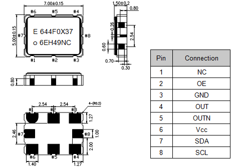
(Unit: mm)
Footprint (Recommended)
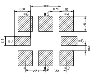
(Unit: mm)
In order to achieve optimum jitter performance, it is recommended that the capacitor (0.1 μF + 10 μF) between VCC and GND pin should be placed as close to the VCC pin as possible.
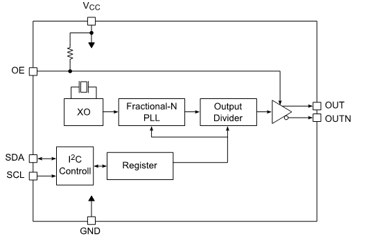
Block diagram
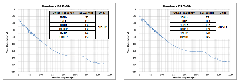
Phase Noise
Phase Jitter
| Offset Frequency | 100 MHz |
125 MHz |
156.25 MHz |
250 MHz |
312.5 MHz |
500 MHz |
625 MHz |
|
|---|---|---|---|---|---|---|---|---|
| Phase jitter *2 Typ. | 12 kHz to 20 MHz | 0.31ps | 0.30ps | 0.26ps | 0.26ps | 0.29ps | 0.28ps | 0.29ps |
*2 In order to achieve optimum jitter performance, it is recommended that the capacitor (0.1 μF + 10 μF) between Vcc and GND pin should be placed as close to the Vcc pin as possible.
