- RTC Top
- What is RTC Modules?
- Epson's RTC Modules
- Features
- Scenes
- RTC Modules for Automotive
- Development Tools
- Videos
RX-4581NB (Built-in SRAM Serial-Interface Real Time Clock Module)
- Built in frequency adjusted 32.768 kHz crystal unit.
- Interface Type
4-wire serial interface
- Operating voltage range
1.6V to 5.5V
- Wide Timekeeper voltage range
1.6V to 5.5V
- Low backup current
0.4µA / 3V(Typ.)
- Built-in SRAM
Built-in 128bit(8bit×16)RAM.
- 32.768kHz frequency output function
C-MOS output With Control Pin
- The various functions include full calendar, alarm, timer.
![]()

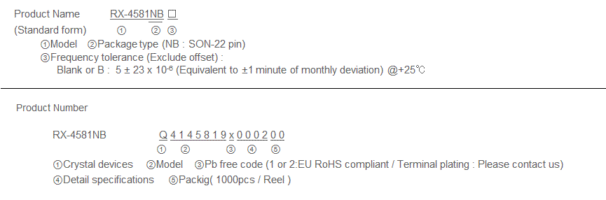
RX-4581NB
Block diagram
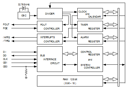
Overview
- Built-in SRAM
- Include 128bit(8bit × 16)RAM.
- Interface Type
- Serial interface in 4lines form.
- * It is possible to make it to 3lines by wired-OR connecting DI and DO pins.
- 32.768kHz frequency output function
- FOUT pin output (C-MOS output), CL=30pF
- FOE pin enables output on/off control.
- Timer function
- Timer function can be set up between 1/4096 second and 4095minutes.
- It is recorded automatic to TF-bit at the time of event
occurrence,and possible to output with /TIRQ pin output
(open-drain output).
- Interrupt function
- Alarm interrupt function , and timer interrupt function.
Specifications *Refer to application manual for details.
Recommend Operating Conditions
| Item | Symbol | Condition | Min. | Typ. | Max. | Unit |
|---|---|---|---|---|---|---|
| Power voltage | VDD | - | 1.6 | 3.0 | 5.5 | V |
| Clock voltage | VCLK | - | 1.6 | 3.0 | 5.5 | V |
| Operating temperature | TOPR | - | -40 | +25 | +85 | °C |
Frequency characteristics
| Item | Symbol | Condition | Rating | Unit |
|---|---|---|---|---|
| Frequency tolerance | Δ f/f | Ta=+25°C VDD=3.0V | 5±23 * | ×10-6 |
| Oscillation start-up time | tSTA | Ta=+25°C VDD=3.0V | 3Max. | s |
* Please ask for tighter tolerance. (Equivalent to ±1minute of monthly deviation)
Current consumption characteristics
*Ta=-40°C to +85°C
| Item | Symbol | Condition | Min. | Typ. | Max. | Unit | |
|---|---|---|---|---|---|---|---|
| Current Consumption |
lBK | CE0,CE1=GND FOE=GND FOUT ;output OFF(Hi-z) |
VDD=5V | 0.6 | 1.2 | µA | |
| VDD=3V | 0.4 | 0.8 | |||||
| l32k | CE0,CE1=GND FOE=VDD FOUT; 32.768kHz output ON CL=30pF |
VDD=5V | 8.0 | 20.0 | µA | ||
| VDD=3V | 5.0 | 12.0 | |||||
Pin function
| Signal Name | Input/Output | Function |
|---|---|---|
| CE0 | Input | The chip enabled input pin 0. (It has a built -in pull-down resistance) |
| CE1 | Input | The chip enabled input pin 1. (It does not have a built -in pull-down resistance) |
| CLK | Input | The shift clock input pin for serial data transfer. |
| Dl | Input | The data input pin for serial data transfer. |
| DO | Output | The data output pin for serial data transfer. |
| FOUT | Output | This pin outputs the reference clock signal at 32.768 kHz (CMOS output). High impedance at the time of output off. |
| FOE | Input | The input pin for the FOUT output control. |
| / AIRQ | Output | The open drain output pin for alarm and time update interrupts. |
| / TIRQ | Output | The open drain output pin for timer interrupt. |
| VDD | - | Connected to a positive power supply. |
| GND | - | Connected to a ground. |
Terminal connection / External dimensions
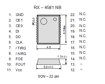
(Unit: mm)
The metal case inside of the molding compound may be exposed on the top or bottom of this product.
This purely cosmetic and does not have any effect on quality, reliability or electrical specs.
Footprint (Recommended)
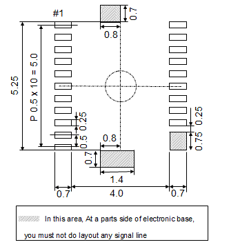
(Unit: mm)
To maintain stable operation, provide a 0.1uF by-pass capacitor
at a location as near as possible to the power source terminal of the crystal product (between Vcc - GND).
