- RTC Top
- What is RTC Modules?
- Epson's RTC Modules
- Features
- Scenes
- RTC Modules for Automotive
- Development Tools
- Videos
RX8010SJ (Low Current Consumption I2C-Bus Interface Real Time Clock Module)
- Built in frequency adjusted 32.768kHz crystal unit.
- Interface Type
I2C-Bus Interface (400kHz)
- Operating voltage range
1.6V to 5.5V
- Wide voltage for time keeping
1.1V to 5.5V
- Low backup current
160nA / 3V(Typ.)
- Frequency output function
C-MOS output or Open-Drain output
- Built-in user RAM
128 bit (8 bit x 16, SRAM)
- The various functions include full calendar, alarm, timer, etc.
- This product is conform to industrial standard SOP8 package, and it can be mounted to the common land pattern.
- Epson prepared Linux driver for development
- https://www5.epsondevice.com/en/information/support/linux_rtc/
The registered trademark Linux® is used pursuant to a sublicense from LMI(Linux Mark Institute)
![]()

RX8010SJ
Block diagram
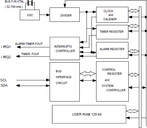
Overview
- Interface Type
- I2C-Bus Interface.(Hi-speed bus specifications 400kHz)
- Frequency output function
- It may select a CMOS or open drain output
- Output frequency can be selected as 32.768kHz, 1024Hz, 1Hz.
- Timer function
- Timer function can be set up between 1/4096 second and 65535 hours.
- Timing period are 1hour, 1min, 64Hz, 4096Hz.
- It is recorded automatic to TF-bit at the time of event occurrence,and possible to output with /IRQ1 or /IRQ2 pin.
- Alarm function
- Alarm function can be set to day of week,day, hour, and minute.
- It is recorded automatic to AF-bit at the time of event occurrence,and possible to output with /IRQ1 pin.
- Built-in RAM
- 128 bit (8 bit x 16 word)
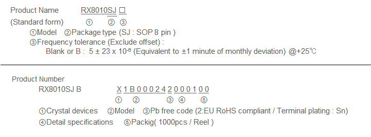
Specifications *Refer to application manual for details.
Recommend Operating Conditions
| Item | Symbol | Condition | Min. | Typ. | Max. | Unit |
|---|---|---|---|---|---|---|
| Power voltage | VDD | - | 1.6 | 3.0 | 5.5 | V |
| Clock voltage | VCLK | - | VLOW | 3.0 | 5.5 | V |
| Operating temperature | TOPR | - | -40 | +25 | +85 | °C |
Frequency characteristics
| Item | Symbol | Condition | Rating | Unit |
|---|---|---|---|---|
| Frequency tolerance |
Δ f/f | Ta=+25°C VDD=3.0V |
5±23 * |
×10-6 |
| Oscillation Start-up time |
tSTA | Ta=+25°C VDD=1.6V~5.5V |
1Max | s |
| Ta=-40°C~+85°C VDD=1.6V~5.5V |
3Max | s |
*Equivalent to ±1 minute of monthly deviation
Current consumption characteristics
Ta=-40°C to +85°C
| Item | Symbol | Conditions | Min. | Typ. | Max. | Unit | |
|---|---|---|---|---|---|---|---|
| Current Consumption | lBK | Input pins are"L" fCLK=0Hz /IRQ1.2=OFF, TSEL2="1" |
VDD=5V | - | - | 350 | nA |
| VDD=3V | - | 160 | 320 | ||||
| l32k | fCLK=0Hz /IRQ1:32.768kHzON, TSEL2="1" |
VDD=5V | - | 5.5 | 7.0 | µA | |
| VDD=3V | - | 3.0 | 4.0 | ||||
Pin function
| Signal Name | Input/ Output |
Function |
|---|---|---|
| SCL | Input | This is a shift clock input pin for serial data transmission. |
| SDA | Bi-directional | This is the data input/output pin for serial data transfer. |
| IRQ1 | Output | This pin outputs interrupt signals ("L" level) for alarm, timer, time update, and 32.768kHz. This is an N-ch open-drain output. |
| /IRQ2 | Output | This pin outputs interrupt signals ("L" level) for timer and FOUT. This is a C-MOS output. |
| VDD | Supply | This is a power-supply pin. |
| GND | Supply | This pin is connected to a ground. |
Terminal connection / External dimensions
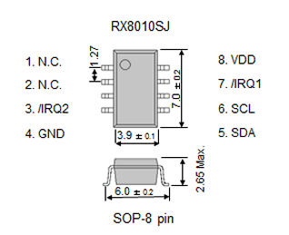
(Unit: mm)
The metal case inside of the molding compound may be exposed on the top or bottom of this product.
This purely cosmetic and does not have any effect on quality, reliability or electrical specs.
Footprint (Recommended)
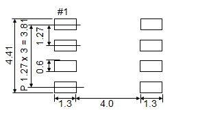
(Unit: mm)
To maintain stable operation, provide a 0.1uF by-pass capacitor
at a location as near as possible to the power source terminal of the crystal product (between Vcc - GND).
