- RTC Top
- What is RTC Modules?
- Epson's RTC Modules
- Features
- Scenes
- RTC Modules for Automotive
- Development Tools
- Videos
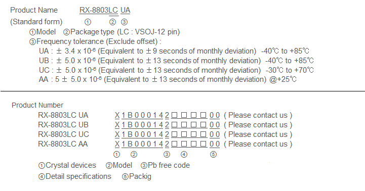
RX-8803LC (Built-in 32.768kHz-DTCXO, High Stability I2C-Bus Interface Real Time Clock Module)
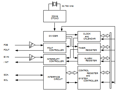
- Built in frequency adjusted 32.768kHz crystal unit and DTCXO.
- 1/100s resolution Time register
- Interface Type
I2C-Bus interface (400kHz)
- Interface voltage range
1.6V to 5.5V
- Temp. compensated voltage range
2.2V to 5.5V
- Clock supply voltage range
1.6V to 5.5V
- Selectable clock output (32.768kHz, 1024Hz, 1Hz)
- The various functions include full calendar, alarm, timer, EVIN input.
- Epson prepared Linux driver for development
- https://www5.epsondevice.com/en/information/support/linux_rtc/
The registered trademark Linux® is used pursuant to a sublicense from LMI(Linux Mark Institute)
![]()

RX-8803LC
Application Manual
(ETM34E-06) ![]() (806kB)
(806kB)
Design Support Data Download
Block diagram
Overview
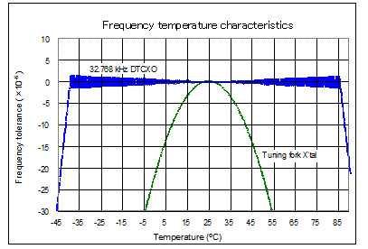
- High Stability
- UA ± 3.4 × 10⁻⁶ / -40°C to +85°C
- (Equivalent to ±9seconds of month deviation)
- UB ± 5.0 × 10⁻⁶ / -40°C to +85°C
- (Equivalent to ±13seconds of month deviation)
- UC ± 5.0 × 10⁻⁶ / -30°C to +70°C
- (Equivalent to ±13seconds of month deviation)
- AA (+5 ± 5.0) × 10-6 / +25°C
- High Resolution:1/100s Time register with capture buffer
- 32.768kHz frequency output function
- FOUT pin output (C-MOS output), CL=30pF
- Output selectable: 32.768kHz, 1024Hz, 1Hz
- The various interrupt
- Timer Function can be set between 1/ 4096second and 4095minutes.
- Alarm Function can be set to day of week, day, hour, or minute.
- EVIN input.
- Time synchronize function with 1PPS signal input
- Register compatibility: upper compatible with RX-8801.
- *It is possible to use it by the terminal connection as 32.768kHz-DTCXO.
Specifications *Refer to application manual for details.
Electrical Characteristics
| Item | Symbol | Condition | Min. | Typ. | Max. | Unit | |
|---|---|---|---|---|---|---|---|
| Operating voltage | VDD | Interface voltage | 1.6 | 3.0 | 5.5 | V | |
| Temp. compensated Voltage | VTEM | Temp. compensated voltage | 2.2 | 3.0 | 5.5 | V | |
| Clock supply voltage | VCLK | - | 1.6 | 3.0 | 5.5 | V | |
| Operating temperature | TOPR | -40 | +25 | +85 | °C | ||
| Stability | Δf/f | UA | Ta = -40°C to +85°C | ±3.4*1 | ×10-6 | ||
| UB | Ta = -40°C to +85°C | ±5.0*2 | |||||
| UC | Ta = -30°C to +70°C | ||||||
| AA | Ta = +25°C | 5 ± 5.0*3 | |||||
| Current consumption (1) | IDD1 | Backup Mode FOE = GND, /INT = VDD FOUT output : OFF |
VDD = 5V | - | 0.75 | 3.4 | µA |
| Current consumption (2) | IDD2 | VDD = 3V | - | 0.75 | 2.1 | ||
*1) Equivalent to ±9 seconds of month deviation.
*2) *3) Equivalent to ±13 seconds of month deviation. (excluding offset)
32.768kHz-DTCXO Frequency temperature characteristics (Example)
Pin function
| Signal Name | Input/Output | Function |
|---|---|---|
| T1(CE) | Input | Use by the manufacture for testing. ( Do not connect externally.) |
| SCL | Input | Serial clock input pin. |
| FOUT | Output | The pin outputs the reference clock signal. ( CMOS output ) |
| VDD | - | Connected to a positive power supply |
| FOE | Input | The input pin for the FOUT output control. |
| EVIN | Input | External event input. ( Do not make this pin OPEN.) |
| / INT | Output | Interrupt output (N-ch. open drain). |
| GND | - | Connected to a ground |
| T2(VPP) | - | Use by the manufacture for testing. ( Do not connect externally.) |
| SDA | I/O | Data input and output pin. |
Terminal connection / External dimensions
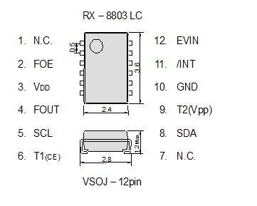
(Unit: mm)
Stop using the glue
Any glue must never use it after soldering LC-package to a circuit board.
This product has glass on the back side of a package.
When glue invasions between circuit board side and glass side, then glass cracks by thermal expansion of glue.
In this case a crystal oscillation stops.Consider glue abolition or glue do not touch to LC-package
Footprint (Recommended)
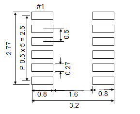
(Unit: mm)
To maintain stable operation, provide a 0.1uF by-pass capacitor
at a location as near as possible to the power source terminal of the crystal product (between Vcc - GND).
