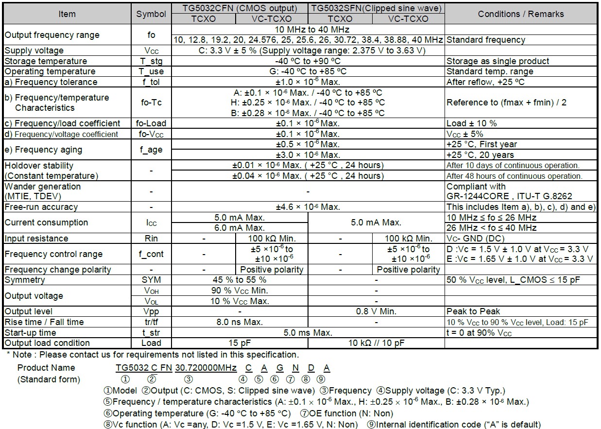
TG5032CFN TCXO / VC-TCXO (ULTRA HIGH STABILITY 4pins terminal type)
- Frequency range
10MHz to 40MHz
- Output waveform
CMOS
- Supply voltage
3.3 V Typ.
- Frequency / temperature characteristics
± 0.1× 10⁻⁶ Max. (-40°C to +85°C)
- Frequency aging
± 3.0× 10⁻⁶ Max. / 20 years
- External dimensions
5.0 × 3.2 × 1.45mm (4pins)
- Applications
Small Cells, Stratum3, SyncE, IEEE1588
- Features
Ultra high stability, Wide temperature range
![]()
![]()

TG5032CFN
Design Support Data Download
Specifications (characteristics)
External dimensions
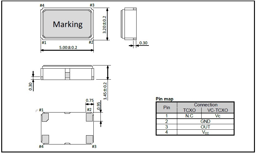
(Unit: mm)
Footprint (Recommended)
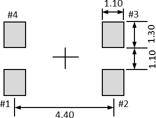
(Unit: mm)
To maintain stable operation, provide a 0.1 µF by-pass capacitor at a location as near as possible to the power source terminal of the crystal product (between VCC - GND).
