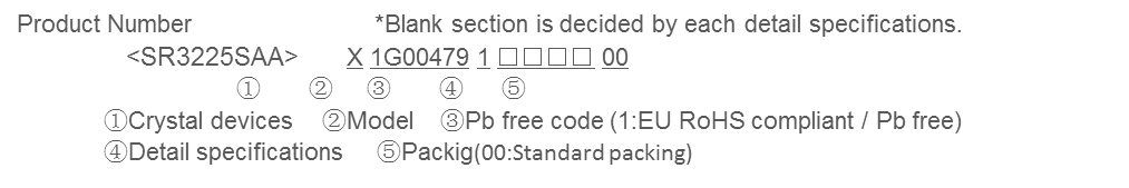
SR3225SAA
RF Transmitter Module
- SR3225SAA is a wireless transmitter module for UHF range.
- Conforms to AEC-Q100.
- Crystal resonator, oscillator, PLL and Power Amp are integrated in 3.2 mm x 2.5 mm ceramic package.
- Application
: Remote Keyless Entry: Passive Entry: Short range radio data transmitter: Garage door opener: Transmitter for RFID tag
![]()
![]()
![]()

SR3225SAA
Block diagram
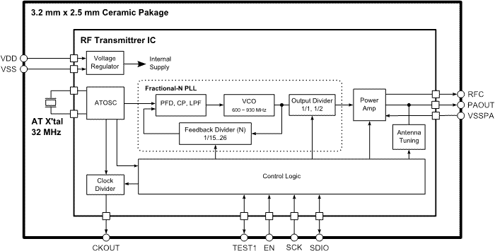
Overview
- Carrier frequency bands
300 MHz to 465 MHz (0.25 kHz Step)600 MHz to 930 MHz (0.49 kHz Step)
- Δ-Σ fractional-N based PLL
- Programmable Power Amp output power:-15 to 11 dBm, 128 steps
- Modulation types: ASK/OOK/FSK with Soft-ASK and/or Soft FSK shaping
- 3-wire/4-wire SPI interface
- SFR (Special Function Register)
- Embedded 32 MHz crystal resonator and oscillation circuit
- Programmable clock output via CKOUT
- Programmable voltage threshold of Under Voltage Detection: 4 steps (1.8 V to 2.4 V)
- Fail-Safe mechanism (PLL Loss of Lock, VCO auto-calibration error, Under Voltage Detection)
Specification (characteristics)
| Parameter | Symbol | Condition | Specification | Unit | ||
|---|---|---|---|---|---|---|
| Min. | Typ. | Max. | ||||
| Supply voltage | VDD | - | 1.8 | 3.0 | 3.6 | V |
| Operation temperature | Ta | - | -40 | - | +85 | ℃ |
| Storage temperature | Tstg | - | -40 | - | +125 | ℃ |
| Supply current Powerdown Mode |
IDDPD | VDD = 3.0 V, Ta = +25 ℃ | - | 20 | 100 | nA |
| Supply current Transmitter-Active Mode |
IDDTMA | FTX = 315 MHz, Pout = 5 dBm, | - | 10.0 | 11.0 | mA |
| FTX = 315 MHz, Pout = 8 dBm, | - | 12.7 | 13.7 | |||
| FTX = 315 MHz, Pout = 10 dBm, | - | 15.0 | 16.0 | |||
| Carrier frequency bands | FTX | - | 300 | - | 465 | MHz |
| 600 | - | 930 | ||||
| ASK Bit rate | RASK | NRZ | - | - | 100 | kbps |
| FSK Bit rate | RFSK | NRZ | - | - | 50 | kbps |
| Crystal frequency tolerance | FTOL | Ta = +25℃, without aging | -2 | - | 2 | ppm |
| Crystal temperature variation | FTC | Ta = -40℃ to +85℃ | -20 | - | 20 | ppm |
| Nominal output power | POUT | Ta = +25℃ VDD = 3.0V FTX = 315 MHz HPWR =1 AM* = 0x3F |
10 | 11 | 12 | dBm |
| Ta = +25℃ VDD = 3.0V FTX = 315 MHz HPWR =0 AM* = 0x01 |
-16 | -15 | -14 | |||
Terminal connection / External dimensions
(Unit:mm)
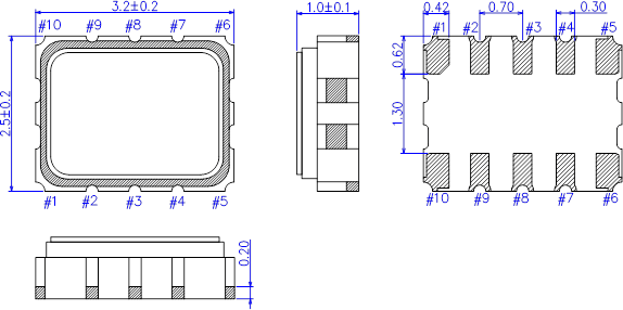
Pin descriptions
| Pin No. | Pin Name | Function |
|---|---|---|
| 1 | TEST1 | Test, Transmission data input or SPI interface data output |
| 2 | EN | Enable input or SPI interface chip select |
| 3 | SCK | SPI interface clock input |
| 4 | SDIO | SPI data input / output or Transmission data input |
| 5 | CKOUT | Clock output |
| 6 | VSSPA | GND for Power Amp |
| 7 | PAOUT | Power Amp output |
| 8 | RFC | RF choke coil connect pin |
| 9 | VDD | Positive power supply |
| 10 | VSS | GND |