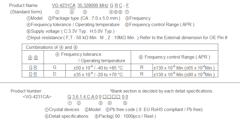
VG-4231CA (Voltage -Controlled Crystal Oscillator (VCXO))
Wide Pull Range
- Frequency range
1MHz to 60MHz
- Supply voltage
3.3V Typ.5.0V Typ.
- Absolute pull range
±80 × 10-6±65 × 10-6
- External dimensions
7.0 × 5.0 × 1.4mm
![]()
![]()

VG-4231CA
Specifications
| Item | Symbol | Specifications | Condition/Remarks | |
|---|---|---|---|---|
| Output frequency range | f0 | 1.000MHz to 60.000MHz | Please contact us for inquiries regarding available frequencies. | |
| Supply voltage | VCC | H : 5.0V ± 0.5V C : 3.3V ± 0.3V |
||
| Control voltage | VC | H : 2.5V ± 2.0V C : 1.65V ± 1.5V |
||
| Storage temperature | T_stg | -40°C to +125°C | Store as bare product. | |
| Operating temperature | T_use | As per below table | ||
| Frequency tolerance | f_tol | As per below table | VC = 2.5V ( **H ) VC = 1.65V ( **C ) |
|
| Current consumption | ICC | H : 20mA Max. C : 10mA Max. |
No load condition | |
| Disable current | I_dis | H : 15mA Max. C : 7mA Max. |
OE = GND | |
| Frequency control range | F_cont | R : ±130 × 10-6 | ||
| Absolute pull range *1 | APR | D : ±80 × 10-6 Min. G : ±65 × 10-6 Min. |
||
| Modulation characteristics | BW | 15kHz Min. | ±3dB (at 1kHz) | |
| Input resistance | Rin | 50kΩ Min. | F or T Type ( Refer to Pin map ) | DC Level |
| 10MΩ Min. ( Only VCC = 3.3V ) | M or Z Type ( Refer to Pin map ) | |||
| Frequency change polarity | - | Positive polarity | ||
| Symmetry | SYM | 40% to 60% | CMOS load: 50% VCC level |
|
| Output voltage | VOH | VCC - 0.4V Min. | IOH = -4mA ( **H ) IOH = -0.8mA ( **C ) |
|
| VOL | 0.4V Max. | IOL = 4mA ( **H ) IOL = 3.2mA ( **C ) |
||
| Output load condition | L_CMOS | 15pF Max. | CMOS load | |
| Input voltage | VIH | 70% VCC Min. | OE terminal | |
| VIL | 30% VCC Max. | |||
| Rise time and Fall time | tr / tf | 4ns Max. | CMOS load: 20% VCC to 80% VCC level |
|
| Start-up time | t_str | 10ms Max. | Time at 90% VCC to be 0s | |
| Frequency aging | f_aging | ±10 × 10-6 Max.*2 | +25°C , 10years | |
*1 Absolute pull range = Frequency control range- (Frequency tolerance + 10years Aging + Free fall + Vibration)
*2 50MHz < f0 ≦ 60MHz : ±15 × 10-6Max.
* Please keep VC pin open or ground while powering up VCC.
External dimensions
OE pin = "H" or "open": Specified frequency output.
OE pin = "L" : Output is high impedance.
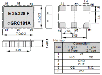
(Unit: mm)
Footprint (Recommended)
To maintain stable operation,
provide a 0.01uF to 0.1uF by-pass capacitor
at a location as near as possible to the
power source terminal of the crystal product
(between Vcc - GND).
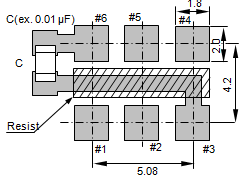
(Unit: mm)
