VG7050CDN VOLTAGE -CONTROLLED CRYSTAL OSCILLATOR(VCXO) OUTPUT:CMOS
- Frequency range
:85 MHz to 170 MHz
- Supply voltage
:3.3 V Typ.
- Absolute Pull Range
:± 50 × 10-6 Min
- Operation temperature
:-40 °C to +85 °C:-40 °C to +105 °C
- External dimensions
:7.0 × 5.0 × 1.5 mm
- Output
:CMOS
- Function
:Output Enable(OE)
(High-Frequency Fundamental)
VG7050CDN
Specifications (characteristics)
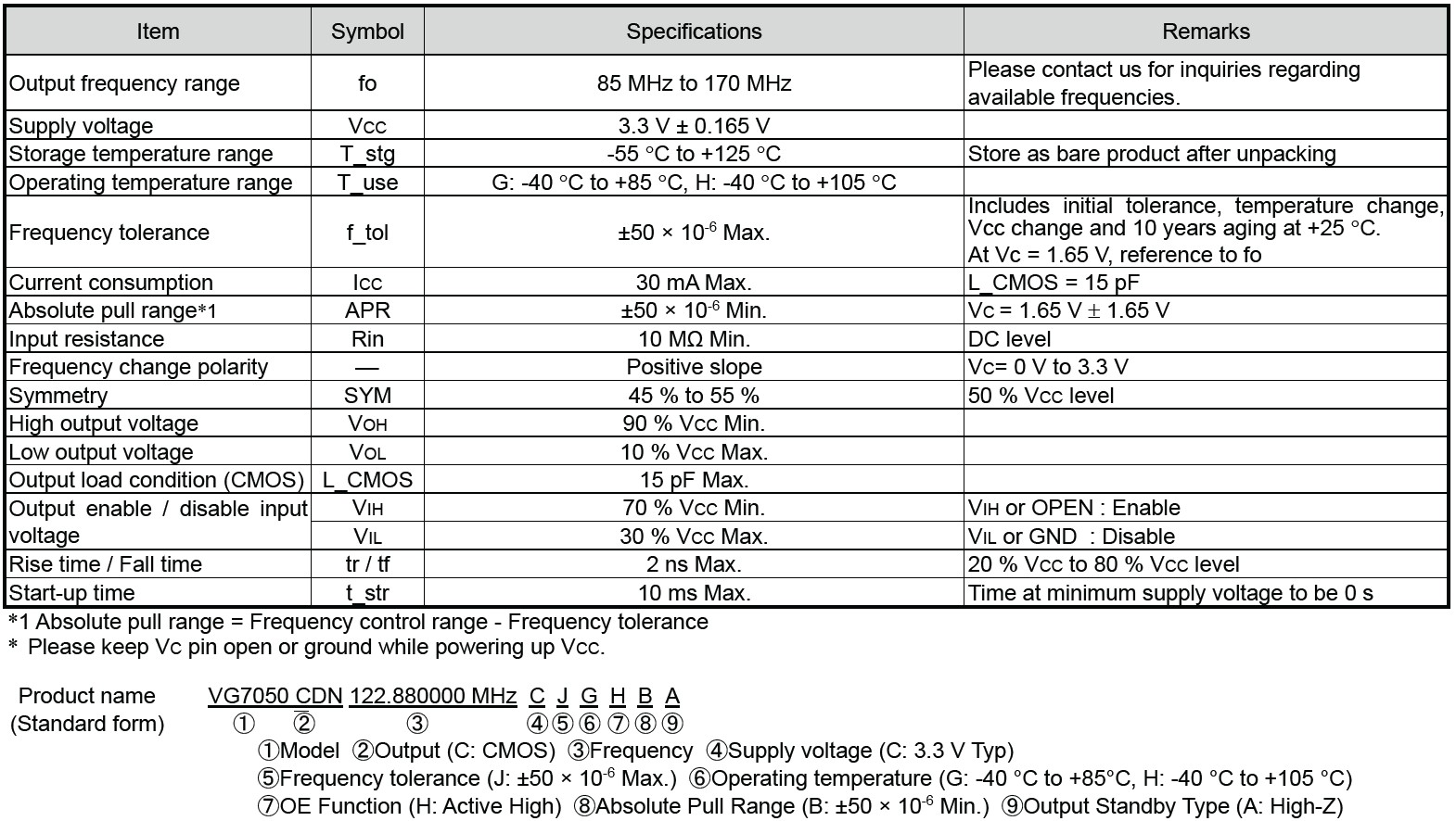
Item | Symbol | Specifications | Conditions / Remarks | ||
---|---|---|---|---|---|
Output frequency range | f0 | 85 MHz to 170 MHz | Please contact us about available frequencies.
|
||
Supply voltage | VCC | 3.3 V ± 0.165 V |
|||
Storage temperature range | T_stg | -55 °C to +125 °C | Storage as single product. | ||
Operating temperature range | T_use | G: -40 °C to +85 °C H: -40 °C to +105 °C |
|||
Current consumption | ICC | 30 mA Max. |
|||
Frequency tolerance | f_tol | ± 50 × 10-6 Max. | Includes initial tolerance, temperature change, VCC change and 10years aging at +25 °C At VC = 1.65 V, reference to f0 |
||
Absolute pull range*1 | APR | ± 50 × 10-6 Min. | VC = 1.65 V ± 1.65 V | ||
Input resistance | Rin | 10 MΩ Min. | DC level | ||
Frequency change polarity |
- | Positive slope | VC = 0 to 3.3 V | ||
Symmetry | SYM | 45 % to 55 % | 50 % VCC level | ||
High output voltage | VOH | VCC - 0.4 V Min. | |||
Low output voltage | VOL | 0.4 V Max. | |||
Output load condition (CMOS) | L_CMOS | 15 pF Max. | |||
High input voltage | VIH | 70 % VCC Min. | VIH or Open : Enable | ||
Low input voltage | VIL | 30 % VCC Max. | VIL or GND : Disable | ||
Rise/Fall times | Tr / Tf | 2 ns Max. | 20 % VCC to 80 % VCC level | ||
Start up time | T_str | 10 ms Max. | Time at minimum supply voltage to be 0 s |
*1 Absolute pull range = Frequency control range - Frequency tolerance.
* Please keep VC pin open or ground while powering up VCC.
Product name (Standard form)
External dimensions
(Unit: mm)
Note.
OE Pin
OE pin = "H" or "Open" : Specified frequency output.
OE pin = "L" : Output is high impedance.
Footprint (Recommended)
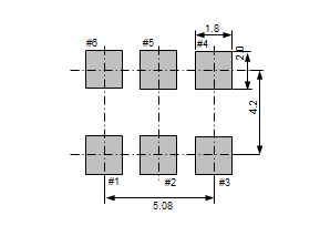
(Unit: mm)
In order to achieve optimum jitter performance, it is recommended that the capacitor (0.1 µF + 10 µF)
between VCC and GND pin should be placed as close to the VCC pin as possible.