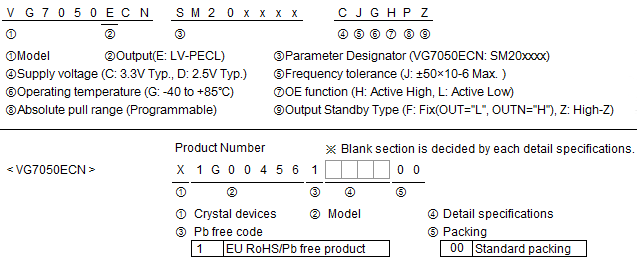
VG7050ECN Programmable Voltage Controlled Oscillator (VCXO) OUTPUT:LV-PECL
- Frequency range
50 MHz ~ 800 MHz(Tuning resolution::2.2~2.8x10⁻⁹)
- Supply voltage
2.5 V / 3.3 V
- External dimensions
7.0 × 5.0 × 1.5 mm (10pins)
- Absolute Pull Range
±0~±180 x 10-6(12 steps selectable)
- Features
- User-specified four startup frequency
- APR and 7-bit I2C address
- User Programming: I2C Interface
- Low jitter PLL technology
- Applications
SONET/SDH, OTN, GbE, Fibre Channel
![]()
![]()

VG7050ECN
Design Support Data Download
Specifications (characteristics)
| Item | Symbol | Specifications | Conditions / Remarks |
|---|---|---|---|
| Output frequency range | f0 | 50 MHz to 800 MHz | It can be changed by I2C |
| Supply voltage | VCC | D:2.5V ±0.125V C:3.3V ±0.33V |
|
| Storage temperature | T_stg | -55°C to +125°C | Storage as single product |
| Operating temperature | T_use | G:-40°C to +85°C, |
|
| Frequency tolerance *1 | f_tol | J: ± 50 × 10-6 Max | Includes frequency aging (10 years) |
| Current consumption | ICC | 90 mA Max. | OE Active, L_ECL=50Ω |
| Disable current | I_dis | 40mA Max. | OE Inactive, Output Standby: Hi-Z mode |
| 70mA Max. | OE Inactive, Output Standby: Fix mode | ||
| Absolute pull range | APR | ±0~±180 x 10-6 | Vc = 1.65 V ± 1.35 V (VCC = 3.3 V) |
| ±0~±180 x 10-6 | Vc = 1.25 V ± 1.00 V (VCC = 2.5 V) |
||
| Control voltage tuning range | Vc | 0~Vcc | |
| Frequency change polarity | - | Positive slope | |
| Symmetry | SYM | 45% ~ 55% | At outputs crossing point |
| Output voltage | VOH | VCC -1.025 V Min. | DC characteristics |
| VOL | VCC -1.62 V Max. | ||
| Output load condition |
L_ECL | 50Ω | Termination to VCC-2.0V |
| Input voltage | VIH | 70% VCC Min. | OE, FSEL0, FSEL1, SDA, and SCL |
| VIL | 30% VCC Max. | ||
| Rise time / Fall time | tr / tf | 400 ps Max. | 20% ~ 80% (VOH- VOL) |
| Start-up time | t_str | 10 ms Max. | Time at minimum supply voltage to be 0 s |
*1. Frequency tolerance includes initial frequency tolerance, temperature variation, supply voltage change, reflow drift and 10 years aging at +25 °C.
Product name (Standard form)
Phase Jitter
| Offset Frequency | 125.00 MHz | 156.25 MHz | 250.00 MHz | 425.00 MHz | 622.08 MHz | 669.33 MHz | 794.73 MHz | |
|---|---|---|---|---|---|---|---|---|
| Phase jitter*2 Typ. |
12 kHz to 20 MHz | 0.30 ps | 0.26 ps | 0.26 ps | 0.25 ps | 0.26 ps | 0.26 ps | 0.26 ps |
| 20 kHz to 50 MHz | 0.30 ps | 0.27 ps | 0.27 ps | 0.26 ps | 0.27 ps | 0.27 ps | 0.27 ps | |
| 50 kHz to 80 MHz | 0.29 ps | 0.27 ps | 0.27 ps | 0.26 ps | 0.27 ps | 0.27 ps | 0.27 ps |
*2. In order to achieve optimum jitter performance, it is recommended that the capacitor (0.1 µF + 10 µF) between Vcc and GND pin should be placed as close to the Vcc pin as possible.
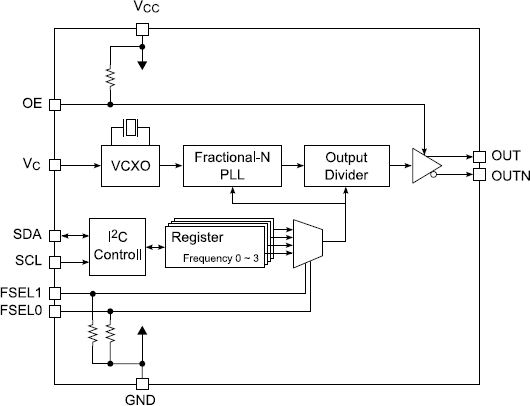
Block diagram
OE Function / OE Standby Type
| OE Function | OE Standby Type | Frequency output OE pin |
Oscillator Stop | |
|---|---|---|---|---|
| OE pin | OUT, OUTNstate |
|||
| H:Active High | Z: High-Z | "H" or "OPEN" | "L" | High Impedance |
| L:Active Low | "L" or "OPEN" | "H" | ||
| H:Active High | F: Fix | "H" or "OPEN" | "L" | OUT="L", OUTN="H" |
| L:Active Low | "L" or "OPEN" | "H" | ||
External dimensions
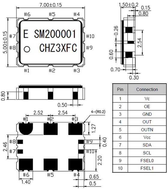
(Unit: mm)
Footprint (Recommended)
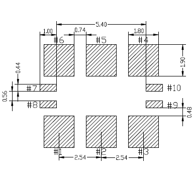
(Unit: mm)
In order to achieve optimum jitter performance, it is recommended that the capacitor (0.1 µF + 10 µF)
between Vcc and GND pin should be placed as close to
the Vcc pin as possible.
