- RTC Top
- What is RTC Modules?
- Epson's RTC Modules
- Features
- Scenes
- RTC Modules for Automotive
- Development Tools
- Videos
REAL TIME CLOCK MODULE
Time stamp function and Low current consumption
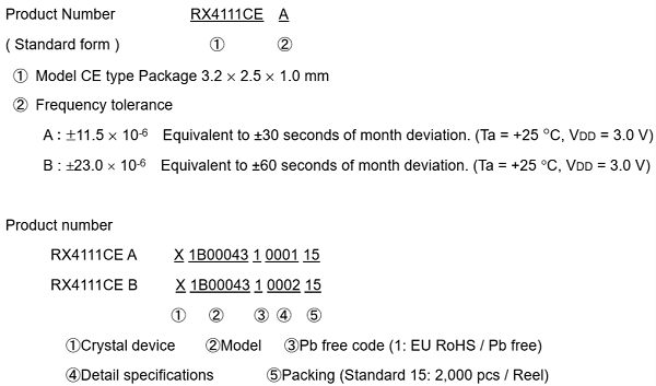
RX4111CE
- - Built in frequency adjusted
32.768 kHz crystal unit - - Interface Type
SPI-Bus interface
I2C-Bus interface Product : RX8111CE Link - - Low backup current
100 nA Typ. / 3 V
- - Operating Temperature
-40 ℃ to +105 ℃
- - Auto power switching function
Automatically switches to backup power supply bymonitoring the VDD voltage
- - Time stamp function
8 times stamped from year to 1/256 seconds.
- - Interrupt output
Wake up every minute or every second
- - Alarm interruption in Day, date,
hour, minute, second - - Auto repeat wakeup timer interruption
- - Self-monitoring interruption
Crystal oscillation stop.VBAT low, VDD low.
- · Links to Driver and Video contents
Click here


RX4111CE
Design Support Data Download
Block diagram
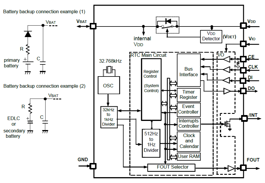
Overview
- Interface Type
- SPI-Bus interface
- Auto power switching function
- The VDD voltage is monitored and it switches to the backup power supply by the automatic operation
- Backup power supply switching voltage 1.2 V Min.
- Clock output function
- Output frequency is selectable from 32.768 kHz, 1024 Hz,1 Hz
- Wakeup timer function
- Selectable from 244 micro second to 32 years(24 bit 1 ch.)
- Timer source clock selectable from 1/60 Hz, 1 Hz, 64 Hz, 4096 Hz
- Auto release after interrupt output from /INT pin at timer completes
- This operation is auto repeat with a selected cycle, it can be used like a watchdog timer
- Time stamp function
- 8 times stamped from year to 1/256 seconds
- The time-stamp trigger inputs from self-monitoring and SPI command
- Alarm function
- It is possible program from year to second
- Self-monitoring interruption
- Crystal oscillation stop. VBAT low, VDD low
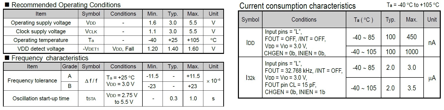
Specifications (characteristics)
Refer to application manual for details
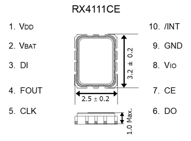
Pin function
Signal Name I / O Function CE input Chip enables input pin CLK input Serial clock input pin DI Input Data input pin DO Output Data output pin FOUT Output Frequency output (CMOS)
(frequency selection: 32.768 kHz, 1024 Hz, 1 Hz)/INT Output Interrupts output by Alarm and Timer events (N-ch. open drain) VDD - Power-supply pin
It can input the voltage unlike VIOVIO - Interface power supply pin
Input to supply the voltage same as a hostVBAT - This is a power supply pin for backup battery
Connect a EDLC, secondary battery, a primary battery
In the backup voltage range, supplied to IC, from this pinGND - Ground pin Terminal connection/External dimensions
(Unit: mm)
Footprint (Recommended)
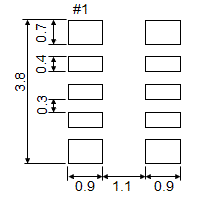
(Unit: mm)
To maintain stable operation, provide a 0.1uF by-pass capacitor
at a location as near as possible to the power source terminal of the crystal product (between Vcc - GND)Links
Video contents: How to use Real Time Clock Module evaluation board(RX8900CE, RX8804CE)
Video contents: RX8111CE: Battery backup switchover function
Video contents: RX8111CE: Time stamp function
Video contents: RX8111CE: Wake up timer function
Video contents: RX4111CE: Battery backup switchover function
Real Time Clock: RX8900CE / RX8804CE Evaluation Tools
Linux® Driver for Real Time Clock Module
The registered trademark Linux® is used pursuant to a sublicense from LMI (Linux Mark Institute) - · Links to Driver and Video contents
